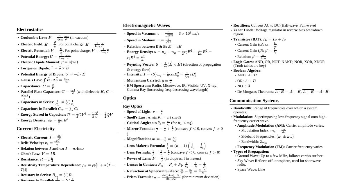
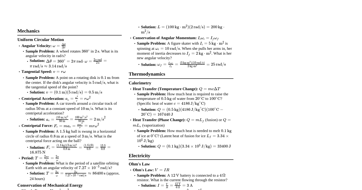
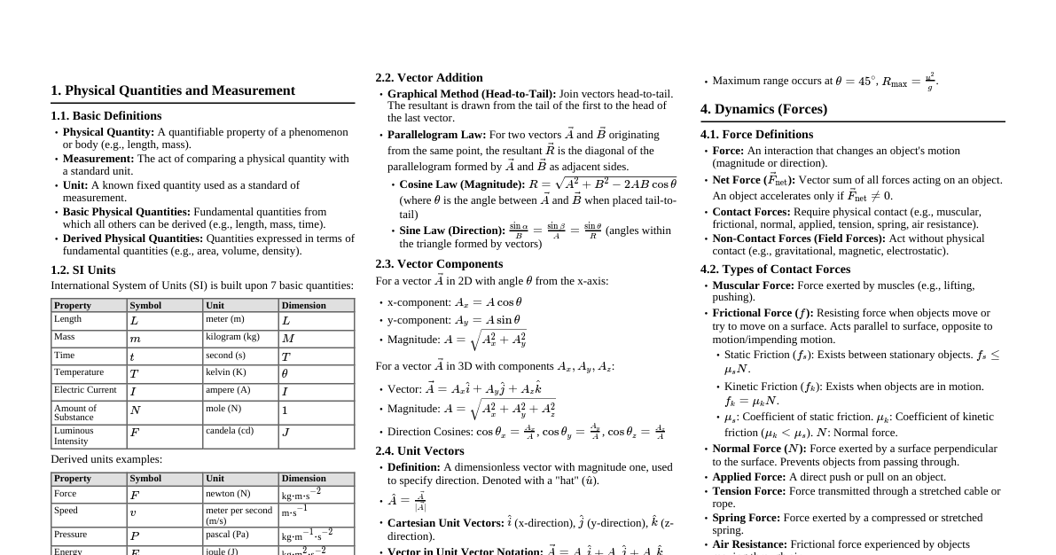
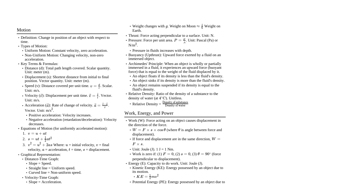
Physics Cheatsheet
Cheatsheet Content
1. Intrinsic Semiconductor A pure semiconductor material (e.g., Si, Ge) with no impurities. At $0$ K, it behaves as an insulator. At room temperature, thermal energy creates electron-hole pairs. Energy Band Diagram Conduction Band ($E_c$): Upper energy band, contains free electrons. Valence Band ($E_v$): Lower energy band, contains holes. Band Gap ($E_g$): Energy difference between $E_c$ and $E_v$. For Si, $E_g \approx 1.12$ eV; for Ge, $E_g \approx 0.67$ eV. In an intrinsic semiconductor, $n_i = p_i$, where $n_i$ is intrinsic electron concentration and $p_i$ is intrinsic hole concentration. The Fermi level ($E_F$) lies approximately in the middle of the band gap. 2. Extrinsic Semiconductor A semiconductor doped with impurities to alter its electrical properties. Doping increases conductivity. n-type Semiconductor Doped with pentavalent impurities (e.g., P, As, Sb) which have 5 valence electrons. Donor atoms donate an extra electron to the conduction band. Majority carriers: electrons; Minority carriers: holes. Donor energy level ($E_d$) is slightly below $E_c$. Fermi level ($E_F$) shifts closer to $E_c$. p-type Semiconductor Doped with trivalent impurities (e.g., B, Al, Ga) which have 3 valence electrons. Acceptor atoms create a "hole" in the valence band. Majority carriers: holes; Minority carriers: electrons. Acceptor energy level ($E_a$) is slightly above $E_v$. Fermi level ($E_F$) shifts closer to $E_v$. 3. Fermi Level ($E_F$) The energy level at which the probability of an electron occupying a state is $1/2$ at any temperature above $0$ K. It represents the chemical potential of electrons. a) Intrinsic Semiconductor $E_F \approx \frac{E_c + E_v}{2} + \frac{3}{4}kT \ln \left(\frac{m_h^*}{m_e^*}\right)$ If $m_e^* = m_h^*$, then $E_F$ is exactly at the middle of the band gap. b) n-type Semiconductor $E_F$ lies between $E_d$ and $E_c$, closer to $E_c$. $E_F = \frac{E_c + E_d}{2} + \frac{kT}{2} \ln \left(\frac{N_d}{N_c}\right)$, where $N_d$ is donor concentration, $N_c$ is effective density of states in conduction band. c) p-type Semiconductor $E_F$ lies between $E_a$ and $E_v$, closer to $E_v$. $E_F = \frac{E_v + E_a}{2} - \frac{kT}{2} \ln \left(\frac{N_a}{N_v}\right)$, where $N_a$ is acceptor concentration, $N_v$ is effective density of states in valence band. 4. Fermi-Dirac Distribution Function Describes the probability that a fermion (like an electron) will occupy a given energy state at a given temperature. $$ F(E) = \frac{1}{1 + e^{(E - E_F)/kT}} $$ $F(E)$: Probability of an energy state $E$ being occupied by an electron. $E$: Energy of the state. $E_F$: Fermi energy level. $k$: Boltzmann constant. $T$: Absolute temperature in Kelvin. Important Properties If $E = E_F$, then $F(E) = 1/2$. If $E If $E > E_F$, $F(E) \approx 0$ (low probability of occupation). At $T = 0$ K: $F(E) = 1$ for $E $F(E) = 0$ for $E > E_F$. The function is symmetric about $E_F$. 5. Hall Effect The production of a voltage difference (Hall voltage) across an electrical conductor, transverse to an electric current in the conductor and a magnetic field perpendicular to the current. Derivation of Hall Coefficient ($R_H$) Consider a current $I$ flowing along the x-axis in a conductor of thickness $t$ and width $w$. A magnetic field $B_z$ is applied along the z-axis. The Lorentz force on charge carriers (electrons) is $F_L = -e(\vec{v}_x \times \vec{B}_z) = -e v_x B_z \hat{y}$. This force pushes electrons to one side, creating a charge imbalance and thus an electric field $E_H$ (Hall field) along the y-axis. At equilibrium, the magnetic force is balanced by the electric force: $F_L + F_E = 0 \implies -e v_x B_z + e E_H = 0$. So, $E_H = v_x B_z$. The current density $J_x = n e v_x$, where $n$ is charge carrier concentration. Thus, $v_x = J_x / (n e)$. Substituting $v_x$: $E_H = \frac{J_x B_z}{n e}$. The Hall coefficient is defined as $R_H = \frac{E_H}{J_x B_z}$. Therefore, $R_H = \frac{1}{n e}$. For holes, $R_H = \frac{1}{p e}$. In general, the sign of $R_H$ indicates the type of charge carrier (negative for electrons, positive for holes). Hall voltage $V_H = E_H w = R_H \frac{I B_z}{t}$. 6. Experimental Setup of Hall Effect A thin rectangular strip of the semiconductor material is used. Current ($I$) is passed longitudinally through the strip (e.g., along the x-axis) via electrodes at the ends. A uniform magnetic field ($B$) is applied perpendicular to the plane of the strip (e.g., along the z-axis). Voltage probes are attached to the sides of the strip (e.g., along the y-axis) to measure the Hall voltage ($V_H$). A voltmeter measures $V_H$. The current is measured by an ammeter, and the magnetic field strength is known. The setup allows for the measurement of $V_H$ for different currents and magnetic field strengths. 7. Applications of Hall Effect Determination of Carrier Type: The sign of the Hall voltage indicates whether the majority carriers are electrons (n-type, $V_H$ negative) or holes (p-type, $V_H$ positive). Measurement of Carrier Concentration: From $R_H = 1/(ne)$ or $1/(pe)$, the carrier concentration $n$ or $p$ can be determined. Measurement of Mobility: Since conductivity $\sigma = ne\mu$, and $R_H = 1/(ne)$, then $\mu = \sigma R_H$. Mobility ($\mu$) can be calculated. Magnetic Field Sensors (Hall Probes): Hall effect sensors are used to measure magnetic field strength. The Hall voltage is directly proportional to the magnetic field. Power Measurement: Used in wattmeters to measure AC power. Current Sensors: Can measure current without direct contact by detecting the magnetic field produced by the current. Position and Speed Sensing: Used in automotive applications (e.g., crankshaft position sensors, anti-lock braking systems). 8. Electrical Conductivity ($\sigma$) A measure of a material's ability to conduct electric current. It is the reciprocal of resistivity ($\rho$). $$ \sigma = \frac{1}{\rho} $$ Derivation for Semiconductor Conductivity In a semiconductor, both electrons and holes contribute to the current. Current density due to electrons: $J_e = n e \mu_e E$, where $n$ is electron concentration, $\mu_e$ is electron mobility, $E$ is electric field. Current density due to holes: $J_h = p e \mu_h E$, where $p$ is hole concentration, $\mu_h$ is hole mobility. Total current density: $J = J_e + J_h = (n e \mu_e + p e \mu_h) E$. Since $J = \sigma E$, we have: $$ \sigma = n e \mu_e + p e \mu_h $$ For intrinsic semiconductors, $n=p=n_i$: $\sigma_i = n_i e (\mu_e + \mu_h)$. For n-type semiconductors, $n \gg p$: $\sigma_n \approx n e \mu_e$. For p-type semiconductors, $p \gg n$: $\sigma_p \approx p e \mu_h$. 9. Mobility of Charge Carriers ($\mu$) The ease with which charge carriers (electrons or holes) can move through a material under the influence of an electric field. It is defined as the drift velocity per unit electric field. $$ \mu = \frac{v_d}{E} $$ $v_d$: Drift velocity of charge carriers. $E$: Applied electric field. Relation between Mobility and Conductivity We know that current density $J = \sigma E$. Also, current density $J = N q v_d$, where $N$ is carrier concentration and $q$ is charge of carrier. For electrons, $J_e = n e v_{de}$. For holes, $J_h = p e v_{dh}$. Substituting $v_d = \mu E$: For electrons: $J_e = n e (\mu_e E) = (n e \mu_e) E$. For holes: $J_h = p e (\mu_h E) = (p e \mu_h) E$. Total current density $J = (n e \mu_e + p e \mu_h) E$. Comparing with $J = \sigma E$, we get: $$ \sigma = n e \mu_e + p e \mu_h $$ This shows that conductivity is directly proportional to the charge carrier concentration and their mobility. 10. Interference due to Thin Film When light falls on a thin film (e.g., oil slick on water, soap bubble), it is reflected from both the top and bottom surfaces. These reflected (or transmitted) rays interfere with each other, producing an interference pattern (colors). Path Difference: The path difference between the two reflected/transmitted rays depends on the film thickness ($t$), refractive index of the film ($\mu$), and angle of incidence ($i$). Phase Change on Reflection: A phase change of $\pi$ (or path change of $\lambda/2$) occurs when light reflects from an optically denser medium. 11. Conditions for Constructive and Destructive Interference (Reflected Light) Consider a thin film of refractive index $\mu$ and thickness $t$, surrounded by a medium of lower refractive index (e.g., air). Light is incident at an angle $i$ and refracts at angle $r$. The optical path difference between the two reflected rays is $2\mu t \cos r$. One reflection (from the top surface) undergoes a $\pi$ phase change (if $\mu_{film} > \mu_{air}$). The other reflection (from the bottom surface) does not (if $\mu_{film} > \mu_{substrate}$). Constructive Interference (Bright Fringe): $$ 2\mu t \cos r = (2n - 1)\frac{\lambda}{2} \quad \text{or} \quad (n + \frac{1}{2})\lambda $$ where $n = 1, 2, 3, \ldots$ Destructive Interference (Dark Fringe): $$ 2\mu t \cos r = n\lambda $$ where $n = 0, 1, 2, 3, \ldots$ Note: If reflections cause two phase changes, or no phase changes, the conditions are reversed. 12. Conditions for Constructive and Destructive Interference (Transmitted Light) The two transmitted rays do not undergo any relative phase change due to reflection. The optical path difference is $2\mu t \cos r$. Constructive Interference (Bright Fringe): $$ 2\mu t \cos r = n\lambda $$ where $n = 0, 1, 2, 3, \ldots$ Destructive Interference (Dark Fringe): $$ 2\mu t \cos r = (2n - 1)\frac{\lambda}{2} \quad \text{or} \quad (n + \frac{1}{2})\lambda $$ where $n = 1, 2, 3, \ldots$ The conditions for transmitted light are exactly opposite to those for reflected light. 13. Newton's Rings Experiment An interference phenomenon observed when a plano-convex lens (with a large radius of curvature) is placed on a flat glass plate. A thin air film of varying thickness is formed between the lens and the plate. When monochromatic light falls normally on this arrangement, concentric bright and dark rings are observed. Light from a source is reflected by a glass plate and falls normally on the air film. Rays reflected from the top surface of the air film (bottom of the lens) and the bottom surface of the air film (top of the glass plate) interfere. The thickness of the air film is zero at the point of contact and gradually increases outwards. A dark spot is observed at the center due to the $\pi$ phase change on reflection from the optically denser glass plate for the second ray. 14. Derivation for Diameter of Newton's Rings Let $R$ be the radius of curvature of the plano-convex lens. If $r$ is the radius of a ring at a point where the air film thickness is $t$, then from geometry ($r^2 = R^2 - (R-t)^2 \approx 2Rt - t^2 \approx 2Rt$ for $t \ll R$). So, $t = r^2 / (2R)$. For Dark Rings: (Condition for reflected light with phase change at one surface) $$ 2\mu t \cos r = n\lambda $$ For air film $\mu=1$, normal incidence $\cos r = \cos 0 = 1$. $$ 2t = n\lambda $$ Substituting $t = r^2 / (2R)$: $$ 2 \left(\frac{r^2}{2R}\right) = n\lambda \implies r^2 = nR\lambda $$ Diameter of the $n^{th}$ dark ring $D_n = 2r_n$: $$ D_n^2 = 4nR\lambda \implies D_n = \sqrt{4nR\lambda} $$ Thus, $D_n \propto \sqrt{n}$. The rings get closer as $n$ increases. For Bright Rings: (Condition for reflected light with phase change at one surface) $$ 2\mu t \cos r = (2n - 1)\frac{\lambda}{2} $$ For air film $\mu=1$, normal incidence $\cos r = 1$. $$ 2t = (2n - 1)\frac{\lambda}{2} $$ Substituting $t = r^2 / (2R)$: $$ 2 \left(\frac{r^2}{2R}\right) = (2n - 1)\frac{\lambda}{2} \implies r^2 = (2n - 1)\frac{R\lambda}{2} $$ Diameter of the $n^{th}$ bright ring $D_n = 2r_n$: $$ D_n^2 = 2(2n - 1)R\lambda \implies D_n = \sqrt{2(2n - 1)R\lambda} $$ Thus, $D_n \propto \sqrt{2n-1}$. 15. Applications of Newton's Rings Determination of Wavelength ($\lambda$): By measuring the diameters of dark rings and knowing $R$, $\lambda$ can be calculated. $$ \lambda = \frac{D_{n+m}^2 - D_n^2}{4mR} $$ Determination of Refractive Index ($\mu$) of a Liquid: By introducing a liquid between the lens and the plate, the ring diameters change, allowing $\mu$ to be calculated. $$ \mu = \frac{D_n^2 (\text{air})}{D_n^2 (\text{liquid})} $$ Testing Optical Surfaces: The regularity and flatness of optical surfaces can be assessed. Irregular rings indicate imperfections. 16. Wedge-Shaped Thin Film A thin film whose thickness varies linearly from zero at one edge to a maximum at the other, forming a wedge (e.g., two glass plates inclined at a small angle $\theta$). When monochromatic light is incident normally, a series of equally spaced straight bright and dark fringes are observed parallel to the line of zero thickness. The optical path difference is $2\mu t$. Condition for Dark Fringe: $2\mu t = n\lambda$. Condition for Bright Fringe: $2\mu t = (2n - 1)\lambda/2$. The fringe spacing $\beta$ (distance between two consecutive bright or dark fringes) is given by: $$ \beta = \frac{\lambda}{2\mu\theta} $$ where $\theta$ is the angle of the wedge in radians. Applications include measuring small angles and gauging the thickness of thin wires. 17. Electric Arc A continuous electrical discharge formed when current flows through a normally non-conductive medium (like air or gas), characterized by high plasma temperature, high current density, and intense light emission. It occurs when the electric field strength exceeds the dielectric breakdown strength of the medium. Properties High Temperature: Arcs can reach temperatures of several thousand Kelvin (e.g., 5,000 K to 20,000 K), ionizing the gas and creating plasma. High Current Density: Current flows through a narrow channel. Negative Resistance Characteristic: As current increases, the voltage drop across the arc decreases due to increased ionization and conductivity. Intense Light Emission: Emits strong light across a broad spectrum due to excited atoms and ions. Noise: Often accompanied by a hissing or buzzing sound. Erosion: Can cause significant erosion of electrodes. Applications Welding: Arc welding uses the heat of the arc to melt and join metals. Lighting: Arc lamps (e.g., carbon arc lamps, xenon arc lamps) are used in projectors, searchlights, and stage lighting due to their high brightness. Furnaces: Electric arc furnaces are used in steelmaking to melt scrap metal. Plasma Torches: Used for cutting and spraying materials. Spectroscopy: Used as an excitation source in atomic emission spectroscopy. Circuit Breakers: High-voltage circuit breakers use arc interruption techniques to safely break current. 18. HRC Fuse (High Rupturing Capacity Fuse) A type of fuse that can safely interrupt a very high short-circuit current without damage to itself or the surrounding electrical circuit. It is widely used in industrial and commercial installations for protection against overcurrents and short circuits. Construction: Consists of a heat-resistant ceramic body with metal end caps. Inside, a silver fuse element is surrounded by a granular filling material (e.g., quartz powder). Working Principle: When an overcurrent flows, the silver fuse element melts and breaks the circuit. The high temperature generated vaporizes the silver. The granular filling material (quenching powder) absorbs the heat and reacts chemically with the silver vapor, forming a high-resistance material that rapidly extinguishes the arc. Advantages: High breaking capacity (can clear large fault currents). Non-deterioration with age. Reliable and consistent performance. Fast operation under short-circuit conditions. Current limiting action (reduces the peak fault current). Applications: Protection of motors, transformers, distribution lines, and industrial equipment in high-power electrical systems.