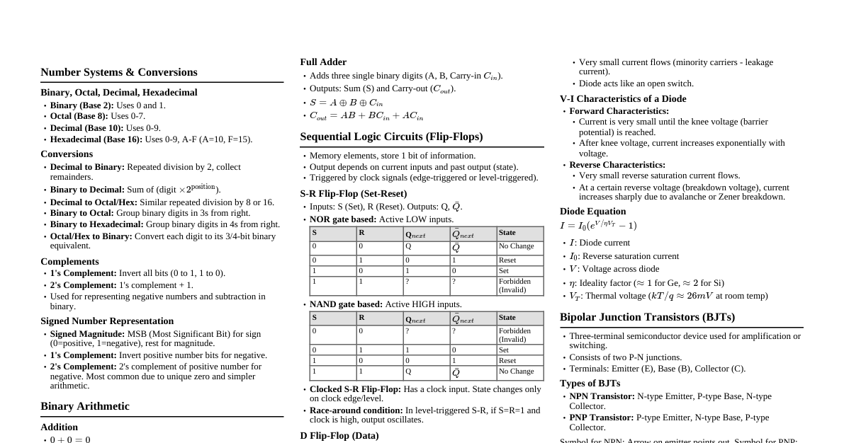
Semiconductor Foundations
Cheatsheet Content
### Day 1: The Bohr Model & Quantum Foundations #### 1.1 The Bohr's Planetary Model The Bohr model, proposed by Niels Bohr in 1913, was a significant step forward in understanding atomic structure, particularly for the hydrogen atom. It addressed some of the shortcomings of earlier models, like Rutherford's model, which predicted that electrons orbiting the nucleus should continuously radiate energy and spiral into the nucleus, making atoms unstable. **Key Postulates of Bohr's Model:** 1. **Stationary Orbits:** Electrons revolve around the nucleus in specific, stable orbits (also called stationary states) without radiating energy. These orbits are associated with definite energy levels. 2. **Quantized Energy Levels:** An electron can only exist in certain discrete orbits, each corresponding to a specific energy level. Electrons cannot exist in between these energy levels. These energy levels are quantized, meaning they can only take on certain discrete values. 3. **Energy Transitions:** Electrons can jump from one stationary orbit to another by absorbing or emitting a photon of energy. * **Absorption:** If an electron absorbs energy equal to the difference between two energy levels, it moves from a lower energy orbit to a higher energy orbit. * **Emission:** When an electron falls from a higher energy orbit to a lower energy orbit, it emits a photon whose energy is exactly equal to the energy difference between the two orbits. The energy of the emitted photon is given by: $$E_{photon} = h\nu = E_{final} - E_{initial}$$ where $h$ is Planck's constant and $\nu$ is the frequency of the photon. 4. **Quantized Angular Momentum:** The angular momentum of an electron in a stationary orbit is also quantized. It can only be an integral multiple of $\frac{h}{2\pi}$ (often denoted as $\hbar$). $$L = mvr = n\frac{h}{2\pi} = n\hbar$$ where $m$ is the electron's mass, $v$ is its velocity, $r$ is the orbit radius, and $n$ is the principal quantum number (n = 1, 2, 3, ...). **Limitations of Bohr's Model:** While revolutionary, Bohr's model had limitations: * It only successfully explained the spectrum of hydrogen and hydrogen-like ions (e.g., He+, Li2+). * It could not explain the spectra of multi-electron atoms. * It failed to explain the fine structure of spectral lines (splitting of lines under high resolution). * It did not account for the Zeeman effect (splitting of spectral lines in the presence of a magnetic field) or the Stark effect (splitting in an electric field). * It treated electrons as particles orbiting in well-defined paths, which is inconsistent with the wave-particle duality of matter. #### 1.2 Discrete Energy Levels vs. Continuous Spectrum This concept is central to understanding how atoms interact with light and forms the basis for spectroscopy. **Continuous Spectrum:** * A continuous spectrum contains all wavelengths of light within a given range, with no gaps. * It is produced by incandescent solids, liquids, or dense gases (e.g., light from a regular incandescent bulb, sunlight after passing through a prism). * The energy of emitted light varies smoothly across a range of frequencies/wavelengths. **Discrete Energy Levels and Line Spectra:** * Atoms, especially in gaseous form, do not emit or absorb light continuously. Instead, they interact with light at very specific, discrete wavelengths, producing **line spectra**. * **Emission Spectrum:** When atoms are excited (e.g., by heating or electrical discharge), their electrons jump to higher energy levels. As these electrons fall back to lower energy levels, they emit photons of specific energies, resulting in bright lines against a dark background. Each element has a unique emission spectrum, acting like a "fingerprint." * **Absorption Spectrum:** When white light passes through a cool gas, the atoms in the gas absorb photons that correspond to the exact energy differences between their allowed energy levels. This results in dark lines appearing in the continuous spectrum at those specific wavelengths. The dark lines in an absorption spectrum correspond exactly to the bright lines in the emission spectrum of the same element. **Why Discrete?** The existence of discrete energy levels is a direct consequence of quantum mechanics. Electrons in an atom are bound to the nucleus, and their possible energy states are quantized due to the wave nature of electrons confined to a small region of space. Just as a guitar string can only vibrate at certain fundamental frequencies and their harmonics, an electron in an atom can only possess specific energy values. #### 1.3 Photoelectric Effect & Photon Concept The photoelectric effect was a crucial phenomenon that challenged classical physics and led to the development of the quantum theory of light. **What is the Photoelectric Effect?** The photoelectric effect is the emission of electrons (called photoelectrons) from a material (usually a metal) when light shines on it. **Observations that Classical Physics Couldn't Explain:** 1. **Existence of a Threshold Frequency:** For a given metal, electrons are only emitted if the incident light has a frequency greater than a certain minimum value, called the **threshold frequency** ($\nu_0$). Below this frequency, no electrons are emitted, no matter how intense the light or how long it shines. Classical wave theory predicted that electron emission should depend on the intensity of light, not its frequency. 2. **Instantaneous Emission:** Electron emission is almost instantaneous (within nanoseconds) once light of the threshold frequency or higher strikes the metal, even at very low light intensities. Classical theory predicted a time delay for electrons to accumulate enough energy from the light wave. 3. **Kinetic Energy of Photoelectrons:** The maximum kinetic energy of the emitted photoelectrons depends only on the frequency of the incident light, not its intensity. Increasing the intensity of light only increases the number of emitted electrons, not their individual kinetic energy. Classical theory predicted that higher intensity light, being a stronger wave, should impart more energy to electrons, leading to higher kinetic energy. **Einstein's Explanation (Photon Concept):** In 1905, Albert Einstein explained the photoelectric effect by extending Planck's idea of quantized energy. He proposed that light itself is not a continuous wave but consists of discrete packets of energy called **photons**. **Key Ideas of Einstein's Photon Theory:** 1. **Light as Photons:** Light consists of individual quanta (photons), each carrying a specific amount of energy given by: $$E = h\nu$$ where $h$ is Planck's constant ($6.626 \times 10^{-34} \text{ J}\cdot\text{s}$) and $\nu$ is the frequency of the light. 2. **One-to-One Interaction:** When a photon strikes the surface of a metal, it behaves like a particle, transferring all its energy to a single electron. 3. **Work Function ($\Phi$):** For an electron to be emitted, it needs a minimum amount of energy to overcome the attractive forces holding it in the metal. This minimum energy is called the **work function** ($\Phi$) of the metal. The work function is specific to each material. 4. **Energy Conservation:** If the energy of the incident photon ($h\nu$) is greater than the work function ($\Phi$), the electron will be emitted. The excess energy is converted into the kinetic energy of the emitted photoelectron. $$h\nu = \Phi + KE_{max}$$ where $KE_{max}$ is the maximum kinetic energy of the emitted electron. This equation is known as **Einstein's Photoelectric Equation**. **Explanation of Observations with Photon Theory:** * **Threshold Frequency:** If $h\nu *Figure 1.1: Bohr Model of the Hydrogen Atom, showing quantized energy levels and electron orbits.* *Figure 1.2: Comparison of continuous, emission, and absorption spectra. Note how absorption lines match emission lines.* *Figure 1.3: Schematic of the Photoelectric Effect. Incident photons strike a metal surface, ejecting electrons if their energy exceeds the work function.* ### Day 2: Atomic Structure to Crystal Formation #### 2.1 Silicon Crystal Structure (Diamond Lattice) Silicon (Si) is the most widely used semiconductor material, and its crystal structure is fundamental to its electronic properties. Silicon atoms arrange themselves in a highly ordered, repeating pattern known as a **crystal lattice**. Specifically, silicon crystallizes in the **diamond cubic structure**. **Key Features of the Diamond Lattice:** * **Unit Cell:** The smallest repeating unit that, when stacked together, forms the entire crystal. The diamond cubic unit cell is a face-centered cubic (FCC) lattice with two atoms per lattice point. * **FCC Basis:** Imagine an FCC structure. In addition to atoms at the corners and face centers, there are four more atoms located within the unit cell. These additional atoms are displaced by $\frac{1}{4}$ of the unit cell diagonal from the FCC lattice points. * **Coordination Number 4:** Each silicon atom is covalently bonded to four nearest neighbor silicon atoms. These bonds are arranged tetrahedrally. * **Tetrahedral Bonding:** The four bonds from a central silicon atom point towards the vertices of a regular tetrahedron. The angle between any two bonds is $109.5^\circ$. * **Open Structure:** Compared to simple cubic or FCC structures, the diamond lattice is relatively open, meaning there is significant empty space within the unit cell. This is due to the directional nature of the covalent bonds. * **Strong Bonds:** The covalent bonds are strong, making silicon a hard material with a high melting point. **Visualizing the Diamond Lattice:** It can be thought of as two interpenetrating FCC lattices, one displaced from the other by a vector $(\frac{a}{4}, \frac{a}{4}, \frac{a}{4})$ where 'a' is the lattice constant (edge length of the unit cell). *Figure 2.1: Diamond cubic unit cell. Note the tetrahedral bonding of each atom.* #### 2.2 Covalent Bonding in Group IV Elements Silicon belongs to Group IV of the periodic table, along with carbon (diamond form), germanium (Ge), and tin (Sn). All these elements share a common characteristic: they have four valence electrons in their outermost shell. **Mechanism of Covalent Bonding:** 1. **Valence Electrons:** Each silicon atom has 4 valence electrons. To achieve a stable electron configuration (like a noble gas, with 8 electrons in the outer shell), silicon atoms share their valence electrons with neighboring atoms. 2. **Shared Pairs:** Each silicon atom forms four covalent bonds with four adjacent silicon atoms. In each covalent bond, one electron comes from the central atom and one from the neighboring atom, forming a shared pair. 3. **Octet Rule:** By sharing electrons, each silicon atom effectively has 8 electrons in its outermost shell (4 of its own + 4 shared from neighbors), satisfying the octet rule and leading to a very stable structure. 4. **Strong and Directional:** Covalent bonds are strong and highly directional. This directional nature is what leads to the specific tetrahedral arrangement and the diamond cubic crystal structure. **Consequences for Semiconductors:** * **Low Conductivity at Low Temperatures:** At absolute zero (0 K), all valence electrons in a perfectly pure silicon crystal are tied up in covalent bonds. There are no free electrons to conduct electricity, making silicon an insulator. * **Semiconducting Behavior:** As temperature increases, some thermal energy can break these covalent bonds, releasing electrons and creating "holes" (a concept we'll explore on Day 3). These free electrons and holes can then conduct electricity, giving silicon its semiconducting properties. * **Doping:** The ability to intentionally introduce impurities (doping) into this covalent bonding structure is what allows us to precisely control the electrical conductivity of semiconductors. #### 2.3 Miller Indices & Crystal Orientations Understanding crystal orientations is crucial for semiconductor device fabrication, as the properties of a material can vary significantly depending on the crystal plane. Miller indices provide a systematic way to describe these planes and directions within a crystal lattice. **What are Miller Indices?** Miller indices are a set of three integers (hkl) that describe the orientation of a crystallographic plane in a crystal lattice. For directions, they are denoted as [uvw]. **Rules for Determining Miller Indices for a Plane (hkl):** 1. **Find Intercepts:** Determine the points where the plane intersects the x, y, and z axes of the unit cell. Express these intercepts in terms of the lattice constant 'a'. If a plane is parallel to an axis, its intercept is at infinity ($\infty$). 2. **Take Reciprocals:** Take the reciprocals of these intercept values. 3. **Clear Fractions:** Multiply the reciprocals by the smallest common integer to clear any fractions, resulting in the smallest set of integers. 4. **Enclose in Parentheses:** Enclose the resulting integers in parentheses, e.g., (hkl). A bar over a number (e.g., $\bar{1}$) indicates a negative intercept. **Example: (100) Plane** * Intercepts: (1a, $\infty$a, $\infty$a) * Reciprocals: ($\frac{1}{1}$, $\frac{1}{\infty}$, $\frac{1}{\infty}$) = (1, 0, 0) * Miller Indices: (100) - This plane cuts the x-axis at 'a' and is parallel to the y and z axes. **Example: (110) Plane** * Intercepts: (1a, 1a, $\infty$a) * Reciprocals: (1, 1, 0) * Miller Indices: (110) **Example: (111) Plane** * Intercepts: (1a, 1a, 1a) * Reciprocals: (1, 1, 1) * Miller Indices: (111) **Miller Indices for Directions [uvw]:** 1. **Vector from Origin:** Draw a vector from the origin to the point (u, v, w) that represents the direction. 2. **Project onto Axes:** Determine the components of this vector along the x, y, and z axes in terms of the lattice constant 'a'. 3. **Clear Fractions:** Multiply by the smallest common integer to clear fractions. 4. **Enclose in Square Brackets:** Enclose the resulting integers in square brackets, e.g., [uvw]. **Key Notations:** * **(hkl):** A specific crystal plane. * `{hkl}`: A family of equivalent planes (e.g., {100} includes (100), (010), (001), ($\bar{1}$00), etc., due to crystal symmetry). * `[uvw]`: A specific crystal direction. * ` `: A family of equivalent directions (e.g., includes [100], [010], [001], etc.). **Importance in Semiconductor Technology:** * **Wafer Orientation:** Silicon wafers are typically cut along specific crystallographic planes, most commonly (100) or (111). * **(100) Wafers:** Preferred for MOS (Metal-Oxide-Semiconductor) devices because the interface between silicon and silicon dioxide ($\text{SiO}_2$) has fewer dangling bonds, leading to better electrical properties. * **(111) Wafers:** Historically used for bipolar junction transistors (BJTs) and some special applications. * **Etching:** The rate and shape of chemical etching processes depend heavily on the crystal orientation. Anisotropic etching, which etches at different rates in different directions, is used to create specific device structures. * **Mechanical Properties:** Mechanical properties like hardness and cleavage also vary with crystal orientation. * **Film Growth:** Epitaxial growth (growing a crystalline film on a crystalline substrate) is highly dependent on matching crystal orientations between the film and the substrate. *Figure 2.2: Examples of common Miller index planes in a cubic crystal system: (100), (110), and (111).* ### Day 3: Introduction to Semiconductors #### 3.1 Definition: Insulator vs. Conductor vs. Semiconductor Materials can be broadly classified into three categories based on their electrical conductivity: conductors, insulators, and semiconductors. This classification is best understood by examining their **band structure**, which describes the allowed energy levels for electrons within the material. **Energy Bands:** In an isolated atom, electrons occupy discrete energy levels. However, when atoms come together to form a solid, these discrete energy levels broaden into **energy bands** due to the interactions between closely spaced atoms. 1. **Valence Band:** This is the highest energy band that is completely or partially filled with electrons at absolute zero temperature (0 K). These electrons are typically involved in bonding and are tightly bound to the atoms. 2. **Conduction Band:** This is the lowest energy band that is empty or partially filled with electrons. Electrons in the conduction band are free to move throughout the material and contribute to electrical current. 3. **Forbidden Band (Band Gap, $E_g$):** This is the energy range between the top of the valence band and the bottom of the conduction band where no electron energy levels are allowed. Electrons cannot exist in the band gap. **Classification by Band Gap:** * **Conductors:** * **Band Structure:** In conductors (e.g., metals like copper, silver, gold), the valence band and conduction band either **overlap** or are very close to each other with no significant band gap ($E_g \approx 0 \text{ eV}$). * **Electron Movement:** This overlap means there are always a large number of free electrons available in the conduction band, even at very low temperatures. These electrons can easily move under the influence of an electric field. * **Conductivity:** Very high electrical conductivity. * **Temperature Dependence:** Conductivity generally decreases with increasing temperature, as increased thermal vibrations scatter electrons more frequently, impeding their flow. * **Insulators:** * **Band Structure:** Insulators (e.g., glass, plastic, wood, rubber) have a very **large band gap** ($E_g > 4 \text{ eV}$, often much larger). The valence band is completely filled, and the conduction band is completely empty at room temperature. * **Electron Movement:** A significant amount of energy is required for an electron to jump from the valence band across the large band gap to the conduction band. At room temperature, thermal energy is usually insufficient to do this. * **Conductivity:** Extremely low electrical conductivity. * **Temperature Dependence:** Conductivity remains very low even at elevated temperatures, as the band gap is too large for thermal energy to bridge effectively. * **Semiconductors:** * **Band Structure:** Semiconductors (e.g., silicon, germanium, gallium arsenide) have a **moderate band gap** ($0.5 \text{ eV} 4 \text{ eV}$ | | **Valence Band** | Partially filled/overlapped | Full at 0K | Full | | **Conduction Band**| Partially filled/overlapped | Empty at 0K | Empty | | **Conductivity** | Very High | Moderate, controllable | Very Low | | **Temp. Effect** | Decreases with T | Increases with T | Remains very low | | **Example** | Copper, Aluminum | Silicon, Germanium | Glass, Plastic | *Figure 3.1: Energy band diagrams for a conductor, semiconductor, and insulator, illustrating the differences in their band gaps.* #### 3.2 Intrinsic Semiconductors (Pure Silicon) An **intrinsic semiconductor** is a semiconductor material in its purest form, with no deliberately added impurities. Pure silicon is an excellent example. **Properties of Intrinsic Silicon:** * **Covalent Bonding:** As discussed on Day 2, each silicon atom forms four covalent bonds with its neighbors, sharing its four valence electrons. At 0 K, all electrons are tightly bound in these covalent bonds. * **Insulator at 0 K:** At absolute zero, there are no free electrons in the conduction band, and the valence band is completely full. Therefore, pure silicon behaves as an insulator. * **Semiconducting Behavior at Higher Temperatures:** As the temperature increases, thermal energy causes the atoms to vibrate. Occasionally, an electron in a covalent bond gains enough energy to break free from the bond and move into the conduction band. * **Creation of Electron-Hole Pairs:** * When an electron breaks a covalent bond and moves to the conduction band, it leaves behind a vacancy in the valence band. This vacancy is called a **hole**. * The electron in the conduction band is now free to move and contribute to current flow. * The hole in the valence band also acts as a charge carrier. While the hole itself doesn't move, an electron from an adjacent bond can jump into the hole, filling it. This makes it appear as if the hole has moved in the opposite direction of the electron. * This simultaneous creation of a free electron and a hole is called **electron-hole pair generation**. **Electron and Hole as Charge Carriers:** * **Electron ($e^-$):** A negatively charged particle (charge = $-q$) that moves in the conduction band. Its movement constitutes an electric current. * **Hole ($h^+$):** A conceptual positively charged particle (charge = $+q$) that moves in the valence band. It represents the absence of an electron in a covalent bond. The movement of a hole is effectively the movement of a "missing negative charge." **Recombination:** Just as electron-hole pairs are generated, they can also recombine. When a free electron in the conduction band encounters a hole in the valence band, the electron can fall back into the hole, releasing energy (often as heat or light). This process is called **recombination**. **Equilibrium:** In an intrinsic semiconductor at a given temperature, there is a continuous process of electron-hole generation and recombination. At thermal equilibrium, the rate of generation equals the rate of recombination, leading to a stable concentration of electrons and holes. #### 3.3 Carrier Generation: Electrons and Holes **Generation Mechanisms:** 1. **Thermal Generation:** This is the most common mechanism in intrinsic semiconductors. As temperature increases, the thermal energy ($k_B T$, where $k_B$ is Boltzmann's constant and $T$ is temperature) becomes sufficient to break covalent bonds. An electron absorbs thermal energy, jumps across the band gap, and moves from the valence band to the conduction band, leaving a hole behind. * The rate of thermal generation depends exponentially on temperature and inversely on the band gap energy. Materials with smaller band gaps (like Germanium, $E_g = 0.67 \text{ eV}$) have higher intrinsic carrier concentrations than those with larger band gaps (like Silicon, $E_g = 1.12 \text{ eV}$) at the same temperature. 2. **Optical Generation (Photoexcitation):** When light (photons) with energy greater than or equal to the band gap energy ($h\nu \ge E_g$) shines on a semiconductor, the photons can be absorbed by electrons in the valence band. This energy excites the electrons, causing them to jump into the conduction band, again creating electron-hole pairs. * This principle is utilized in photodiodes, solar cells, and photodetectors. 3. **High-Energy Particle Impact:** High-energy particles (e.g., alpha particles, cosmic rays) can also impart enough energy to electrons to break bonds and create electron-hole pairs. This is relevant in radiation detectors. **Electron-Hole Pair (EHP):** The fundamental unit of charge carriers generated in a semiconductor is an electron-hole pair. In an intrinsic semiconductor, electrons and holes are always created in pairs, so the concentration of electrons ($n$) is equal to the concentration of holes ($p$). This is denoted as the **intrinsic carrier concentration**, $n_i$. $$n = p = n_i$$ **Significance:** The ability to generate and control these charge carriers (electrons and holes) is what makes semiconductors so versatile. By manipulating the generation rate (e.g., with light) or by intentionally introducing impurities (doping), we can control the conductivity and create various electronic devices. The concept of holes as mobile positive charge carriers is crucial for understanding current flow in semiconductors and the operation of p-n junctions and transistors. #### 3.4 Essential Diagrams *Figure 3.2: Illustration of electron-hole pair generation in an intrinsic semiconductor due to thermal energy. An electron breaks free from a covalent bond, leaving a hole.* *Figure 3.3: Diagram showing the movement of a hole. An electron jumps into a hole, making it appear as if the positive hole has moved in the opposite direction.* ### Day 4: Carrier Statistics & Thermal Effects #### 4.1 Thermal Equilibrium and Carrier Concentration **Thermal Equilibrium:** In semiconductor physics, **thermal equilibrium** refers to a state where the material's properties (like temperature, carrier concentrations, and energy distributions) are constant over time and there are no external forces (like electric fields, light, or temperature gradients) acting on it. In this state, the rate of electron-hole pair generation is exactly balanced by the rate of electron-hole recombination. * **Generation Rate (G):** The rate at which electron-hole pairs are created per unit volume per unit time. In intrinsic semiconductors, this is primarily due to thermal energy at room temperature. * **Recombination Rate (R):** The rate at which electrons and holes annihilate each other. This rate is proportional to the product of electron and hole concentrations ($n \cdot p$). At thermal equilibrium: $G = R$. **Carrier Concentration:** The number of charge carriers (electrons and holes) per unit volume is called the **carrier concentration**. In an intrinsic semiconductor at thermal equilibrium, the concentration of free electrons ($n_0$) in the conduction band is equal to the concentration of holes ($p_0$) in the valence band. $$n_0 = p_0 = n_i$$ where $n_i$ is the **intrinsic carrier concentration**. The subscript '0' denotes thermal equilibrium conditions. **Fermi Level ($E_F$):** The Fermi level is a crucial concept in semiconductor physics. It represents the energy level at which there is a 50% probability of finding an electron, assuming an available state at that energy. * **Significance:** The position of the Fermi level relative to the conduction band edge ($E_C$) and valence band edge ($E_V$) dictates the distribution of electrons and holes. * **Intrinsic Semiconductor:** In an intrinsic semiconductor, the Fermi level ($E_{Fi}$) lies approximately in the middle of the band gap. $$E_{Fi} \approx \frac{E_C + E_V}{2}$$ This position reflects the equal probability of finding electrons and holes. **Fermi-Dirac Distribution Function:** The probability of an electron occupying an energy state $E$ at a given temperature $T$ is described by the Fermi-Dirac distribution function: $$f(E) = \frac{1}{1 + e^{(E - E_F)/k_B T}}$$ where $k_B$ is Boltzmann's constant. * If $E = E_F$, then $f(E) = 0.5$ (50% probability). * If $E > E_F$, then $f(E) 0.5$. The probability approaches 1 as $E$ moves below $E_F$. For holes, the probability of an energy state $E$ being empty (i.e., a hole existing) is $1 - f(E)$. #### 4.2 Intrinsic Carrier Density ($n_i$) The intrinsic carrier density ($n_i$) is one of the most fundamental parameters of a semiconductor. It represents the concentration of electrons (and holes) in a pure, undoped semiconductor at thermal equilibrium. **Formula for Intrinsic Carrier Concentration:** The intrinsic carrier concentration ($n_i$) is given by the following equation: $$n_i = \sqrt{N_C N_V} \cdot e^{-E_g / (2k_B T)}$$ where: * $N_C$: Effective density of states in the conduction band. It represents the total number of available states in the conduction band near $E_C$. * $N_V$: Effective density of states in the valence band. It represents the total number of available states in the valence band near $E_V$. * $E_g$: Band gap energy of the semiconductor (in electron volts, eV). * $k_B$: Boltzmann's constant ($8.617 \times 10^{-5} \text{ eV/K}$ or $1.38 \times 10^{-23} \text{ J/K}$). * $T$: Absolute temperature in Kelvin (K). **The terms $N_C$ and $N_V$ can be expressed as:** $$N_C = 2 \left( \frac{2\pi m_e^* k_B T}{h^2} \right)^{3/2}$$ $$N_V = 2 \left( \frac{2\pi m_h^* k_B T}{h^2} \right)^{3/2}$$ where: * $m_e^*$: Effective mass of an electron in the conduction band. * $m_h^*$: Effective mass of a hole in the valence band. * $h$: Planck's constant. **Combining these, a more complete expression for $n_i$ is:** $$n_i = 2 \left( \frac{k_B T}{2\pi \hbar^2} \right)^{3/2} (m_e^* m_h^*)^{3/4} e^{-E_g / (2k_B T)}$$ or, more simply, often approximated as: $$n_i = A T^{3/2} e^{-E_g / (2k_B T)}$$ where A is a material-specific constant. **Key Observations from the $n_i$ Formula:** 1. **Exponential Dependence on Temperature:** The most dominant factor is the exponential term. $n_i$ increases very rapidly with increasing temperature. This is because higher temperatures provide more thermal energy to break covalent bonds and generate electron-hole pairs. 2. **Inverse Exponential Dependence on Band Gap:** Materials with smaller band gaps ($E_g$) will have a significantly higher $n_i$ at a given temperature compared to materials with larger band gaps. This explains why Ge ($E_g = 0.67 \text{ eV}$) has a much higher $n_i$ than Si ($E_g = 1.12 \text{ eV}$) at room temperature. 3. **Weak Power Law Dependence on Temperature:** The $T^{3/2}$ term also contributes to the increase in $n_i$ with temperature, but its effect is much weaker than the exponential term. **Typical Values at Room Temperature (300 K):** * For Silicon (Si): $n_i \approx 1 \times 10^{10} \text{ cm}^{-3}$ * For Germanium (Ge): $n_i \approx 2.4 \times 10^{13} \text{ cm}^{-3}$ * For Gallium Arsenide (GaAs): $n_i \approx 1.8 \times 10^6 \text{ cm}^{-3}$ These values highlight the vast difference in intrinsic carrier concentrations among different semiconductor materials, primarily due to their band gap energies. #### 4.3 Temperature Dependence of Conductivity The electrical conductivity ($\sigma$) of a semiconductor is directly related to the concentration and mobility of its charge carriers. $$\sigma = q(n\mu_n + p\mu_p)$$ where: * $q$: Elementary charge ($1.602 \times 10^{-19} \text{ C}$). * $n$: Concentration of free electrons. * $p$: Concentration of holes. * $\mu_n$: Mobility of electrons (how easily electrons move in an electric field). * $\mu_p$: Mobility of holes. **In an Intrinsic Semiconductor:** Since $n = p = n_i$, the conductivity equation becomes: $$\sigma_i = q n_i (\mu_n + \mu_p)$$ **Temperature Effects on Conductivity:** 1. **Carrier Concentration ($n_i$):** As discussed, $n_i$ increases exponentially with temperature. This is the dominant factor determining the temperature dependence of conductivity in intrinsic semiconductors. 2. **Carrier Mobility ($\mu_n, \mu_p$):** Mobility generally decreases with increasing temperature. This is because increased thermal vibrations of the crystal lattice atoms cause more scattering of the charge carriers, impeding their movement. Mobility typically decreases with temperature as $T^{-m}$, where $m$ is between 1.5 and 2.5. **Overall Effect:** Despite the decrease in mobility, the exponential increase in intrinsic carrier concentration ($n_i$) with temperature is much stronger. Therefore, the net effect is that the electrical conductivity of an intrinsic semiconductor **increases significantly with increasing temperature**. **Contrast with Conductors:** Recall that for conductors, conductivity typically decreases with increasing temperature. This is because in conductors, the number of charge carriers is already very high and nearly constant. The only significant temperature effect is the increased scattering, which reduces mobility and thus conductivity. **Practical Implications:** * **Temperature Sensitivity:** Semiconductor devices are inherently sensitive to temperature changes. This is why many electronic components have specified operating temperature ranges. * **Thermal Runaway:** In some power devices, if not properly designed and cooled, an increase in temperature can lead to a runaway increase in current, potentially damaging the device. * **Thermistors:** The strong temperature dependence of semiconductor resistance is utilized in thermistors, which are temperature-sensing devices. **Summary of Temperature Dependence:** * **Intrinsic Semiconductors:** As T increases, $n_i$ increases exponentially (dominant effect), $\mu$ decreases (weaker effect), leading to **$\sigma$ increasing exponentially with T**. * **Conductors:** As T increases, carrier concentration is constant, $\mu$ decreases, leading to **$\sigma$ decreasing linearly with T**. #### 4.4 Essential Diagrams *Figure 4.1: Energy band diagram for an intrinsic semiconductor showing the Fermi level ($E_{Fi}$) approximately in the middle of the band gap.* *Figure 4.2: Schematic plot of intrinsic semiconductor conductivity vs. temperature, illustrating the exponential increase.* ### Day 5: Problem Session - Carrier Calculations #### 5.1 Calculating $n_i$ at Different Temperatures **Recall the formula for intrinsic carrier concentration:** $$n_i = N_C N_V e^{-E_g / (2k_B T)}$$ where $N_C = 2 \left( \frac{2\pi m_e^* k_B T}{h^2} \right)^{3/2}$ and $N_V = 2 \left( \frac{2\pi m_h^* k_B T}{h^2} \right)^{3/2}$ A more practical form for calculations is often: $$n_i = A T^{3/2} e^{-E_g / (2k_B T)}$$ where A is a material-specific constant. For Silicon, a commonly used value for the pre-exponential factor $N_C N_V$ is approximately $3.1 \times 10^{32} \text{ cm}^{-6}$ at 300K, and $E_g = 1.12 \text{ eV}$. Another common approximation for $n_i$ at a given temperature $T$ (in K): $$n_i^2 = (1.08 \times 10^{31} T^3) e^{-1.21/(k_B T)}$$ where $1.21$ is the bandgap for Si at 0K, which is slightly different from 1.12eV at 300K. For consistency, we will use $E_g = 1.12 \text{ eV}$ for Si at 300K. **Constants to Use:** * Boltzmann's constant, $k_B = 8.617 \times 10^{-5} \text{ eV/K}$ * Band gap for Silicon, $E_g = 1.12 \text{ eV}$ (at 300 K) * Effective density of states for Silicon at 300K: * $N_C = 2.8 \times 10^{19} \text{ cm}^{-3}$ * $N_V = 1.04 \times 10^{19} \text{ cm}^{-3}$ **Problem 1: Calculate $n_i$ for Silicon at 300 K.** **Solution:** Given: $T = 300 \text{ K}$, $E_g = 1.12 \text{ eV}$, $k_B = 8.617 \times 10^{-5} \text{ eV/K}$ $N_C = 2.8 \times 10^{19} \text{ cm}^{-3}$, $N_V = 1.04 \times 10^{19} \text{ cm}^{-3}$ First, calculate the exponential term: $\frac{E_g}{2k_B T} = \frac{1.12 \text{ eV}}{2 \times (8.617 \times 10^{-5} \text{ eV/K}) \times 300 \text{ K}} = \frac{1.12}{0.051702} \approx 21.662$ $e^{-E_g / (2k_B T)} = e^{-21.662} \approx 3.53 \times 10^{-10}$ Now, calculate $n_i$: $n_i = \sqrt{N_C N_V} \cdot e^{-E_g / (2k_B T)}$ $n_i = \sqrt{(2.8 \times 10^{19}) \times (1.04 \times 10^{19})} \times (3.53 \times 10^{-10})$ $n_i = \sqrt{2.912 \times 10^{38}} \times (3.53 \times 10^{-10})$ $n_i = (1.706 \times 10^{19}) \times (3.53 \times 10^{-10})$ $n_i \approx 6.02 \times 10^9 \text{ cm}^{-3}$ *Note: The commonly cited value for Si $n_i$ at 300 K is about $1 \times 10^{10} \text{ cm}^{-3}$. The slight difference here can be attributed to using specific values for $N_C$, $N_V$ and $E_g$ at 300K, which vary slightly in literature. The key is the magnitude and the exponential dependence.* **Problem 2: Calculate $n_i$ for Silicon at 400 K.** **Solution:** Given: $T = 400 \text{ K}$, $E_g = 1.12 \text{ eV}$, $k_B = 8.617 \times 10^{-5} \text{ eV/K}$ *Note: $N_C$ and $N_V$ are also temperature-dependent ($T^{3/2}$). For a more precise calculation, one would update $N_C$ and $N_V$ for 400 K. However, for a simpler estimate, we can use the 300K values or use the $A T^{3/2}$ form if A is given.* Let's use the $N_C, N_V$ values adjusted for $T^{3/2}$ dependence: $N_C(400K) = N_C(300K) \times (\frac{400}{300})^{3/2} = 2.8 \times 10^{19} \times (1.333)^{1.5} \approx 2.8 \times 10^{19} \times 1.539 \approx 4.31 \times 10^{19} \text{ cm}^{-3}$ $N_V(400K) = N_V(300K) \times (\frac{400}{300})^{3/2} = 1.04 \times 10^{19} \times 1.539 \approx 1.60 \times 10^{19} \text{ cm}^{-3}$ Now, calculate the exponential term: $\frac{E_g}{2k_B T} = \frac{1.12 \text{ eV}}{2 \times (8.617 \times 10^{-5} \text{ eV/K}) \times 400 \text{ K}} = \frac{1.12}{0.068936} \approx 16.246$ $e^{-E_g / (2k_B T)} = e^{-16.246} \approx 8.78 \times 10^{-8}$ Now, calculate $n_i$: $n_i = \sqrt{N_C(400K) N_V(400K)} \cdot e^{-E_g / (2k_B T)}$ $n_i = \sqrt{(4.31 \times 10^{19}) \times (1.60 \times 10^{19})} \times (8.78 \times 10^{-8})$ $n_i = \sqrt{6.896 \times 10^{38}} \times (8.78 \times 10^{-8})$ $n_i = (2.626 \times 10^{19}) \times (8.78 \times 10^{-8})$ $n_i \approx 2.30 \times 10^{12} \text{ cm}^{-3}$ **Observation:** Notice how $n_i$ increases by several orders of magnitude (from $\sim 10^9$ to $\sim 10^{12}$) for a relatively small temperature increase (from 300 K to 400 K). This highlights the strong exponential dependence of $n_i$ on temperature. #### 5.2 Simple Conductivity Problems **Recall the intrinsic conductivity formula:** $$\sigma_i = q n_i (\mu_n + \mu_p)$$ where $q = 1.602 \times 10^{-19} \text{ C}$. **Typical Mobility Values for Silicon at 300 K:** * Electron mobility, $\mu_n \approx 1350 \text{ cm}^2/\text{V}\cdot\text{s}$ * Hole mobility, $\mu_p \approx 480 \text{ cm}^2/\text{V}\cdot\text{s}$ **Problem 3: Calculate the intrinsic conductivity of Silicon at 300 K.** **Solution:** Using $n_i \approx 1 \times 10^{10} \text{ cm}^{-3}$ (a common textbook value for Si at 300K for simplicity). Given: $n_i = 1 \times 10^{10} \text{ cm}^{-3}$, $q = 1.602 \times 10^{-19} \text{ C}$ $\mu_n = 1350 \text{ cm}^2/\text{V}\cdot\text{s}$, $\mu_p = 480 \text{ cm}^2/\text{V}\cdot\text{s}$ $\sigma_i = q n_i (\mu_n + \mu_p)$ $\sigma_i = (1.602 \times 10^{-19} \text{ C}) \times (1 \times 10^{10} \text{ cm}^{-3}) \times (1350 + 480 \text{ cm}^2/\text{V}\cdot\text{s})$ $\sigma_i = (1.602 \times 10^{-19}) \times (1 \times 10^{10}) \times (1830)$ $\sigma_i = 2931.66 \times 10^{-9} \text{ S/cm}$ $\sigma_i \approx 2.93 \times 10^{-6} \text{ S/cm}$ **Problem 4: If the resistance of a 1 cm long, 1 mm x 1 mm intrinsic silicon bar at 300 K is $R$. What would happen to its resistance if the temperature increases to 400 K? (Qualitative analysis)** **Solution:** * **Resistance and Conductivity:** Resistance $R = \rho \frac{L}{A} = \frac{1}{\sigma} \frac{L}{A}$, where $\rho$ is resistivity, $L$ is length, and $A$ is cross-sectional area. So, resistance is inversely proportional to conductivity ($R \propto 1/\sigma$). * **Temperature Effect on Conductivity:** From Day 4 and Problem 2, we know that the intrinsic carrier concentration ($n_i$) increases significantly with temperature. While mobility decreases, the increase in $n_i$ is exponentially dominant. Therefore, the conductivity ($\sigma_i$) of intrinsic silicon **increases significantly** when the temperature rises from 300 K to 400 K. * **Effect on Resistance:** Since conductivity increases, the resistance of the silicon bar will **decrease significantly**. **Problem 5: A semiconductor material has $n_i = 10^{13} \text{ cm}^{-3}$ at 300 K. If its electron mobility is $1000 \text{ cm}^2/\text{V}\cdot\text{s}$ and hole mobility is $400 \text{ cm}^2/\text{V}\cdot\text{s}$, calculate its intrinsic resistivity.** **Solution:** First, calculate intrinsic conductivity $\sigma_i$: $q = 1.602 \times 10^{-19} \text{ C}$ $n_i = 10^{13} \text{ cm}^{-3}$ $\mu_n = 1000 \text{ cm}^2/\text{V}\cdot\text{s}$ $\mu_p = 400 \text{ cm}^2/\text{V}\cdot\text{s}$ $\sigma_i = q n_i (\mu_n + \mu_p)$ $\sigma_i = (1.602 \times 10^{-19}) \times (10^{13}) \times (1000 + 400)$ $\sigma_i = (1.602 \times 10^{-19}) \times (10^{13}) \times (1400)$ $\sigma_i = 2242.8 \times 10^{-6} \text{ S/cm}$ $\sigma_i \approx 2.24 \times 10^{-3} \text{ S/cm}$ Now, calculate intrinsic resistivity $\rho_i = 1/\sigma_i$: $\rho_i = \frac{1}{2.24 \times 10^{-3} \text{ S/cm}}$ $\rho_i \approx 446 \text{ } \Omega\cdot\text{cm}$ #### 5.3 Real-World Implications The calculations and concepts related to carrier statistics and thermal effects have profound implications for the design, performance, and reliability of semiconductor devices. 1. **Device Performance and Reliability:** * **Temperature Sensitivity:** As shown, the intrinsic carrier concentration $n_i$ is extremely sensitive to temperature. This means that the electrical properties (current, resistance) of semiconductor devices change significantly with temperature. * **Leakage Current:** In p-n junction diodes and transistors, $n_i$ contributes to reverse leakage current. Higher temperatures lead to higher $n_i$, which in turn increases leakage currents, degrading device performance and increasing power consumption. * **Thermal Runaway:** In high-power devices, if cooling is inadequate, increased temperature can lead to increased current, which generates more heat, leading to further current increase—a positive feedback loop known as thermal runaway, potentially destroying the device. 2. **Material Selection:** * **Band Gap Choice:** The band gap ($E_g$) is a critical factor. Materials with larger band gaps (e.g., GaAs, GaN, SiC) have much lower $n_i$ at a given temperature. This makes them suitable for high-temperature and high-power applications, as their intrinsic properties are less affected by thermal generation. * **Silicon vs. Germanium:** Germanium has a smaller band gap than silicon, leading to a much higher $n_i$ at room temperature. This made early germanium transistors very noisy and prone to thermal instability, leading to silicon's dominance in modern electronics. 3. **Doping for Control:** * In practical devices, semiconductors are **doped** (intentionally adding impurities) to create extrinsic semiconductors (n-type or p-type). Doping creates a large imbalance between electron and hole concentrations, making one type of carrier dominant. * The conductivity of doped semiconductors is primarily determined by the doping concentration, which is far greater than $n_i$ at room temperature. This makes the conductivity of doped semiconductors much less sensitive to temperature changes (compared to intrinsic semiconductors) over their operating range, as long as the temperature is not so high that $n_i$ becomes comparable to the doping concentration. 4. **Sensor Applications:** * **Thermistors:** The strong temperature dependence of semiconductor resistance is harnessed in thermistors, which are used for precise temperature measurement and control. * **Photodetectors:** The optical generation of electron-hole pairs (where $n_i$ contributes to dark current) is the basis of photodetectors and solar cells. Understanding $n_i$ helps in designing devices with optimal sensitivity and low noise. 5. **Device Modeling and Simulation:** * Accurate calculation of $n_i$ and its temperature dependence is essential for simulating the behavior of semiconductor devices across various operating conditions. This allows engineers to predict performance and optimize designs before fabrication. In summary, the intrinsic carrier concentration ($n_i$) and its exponential dependence on temperature are fundamental to understanding the behavior of semiconductors. While intrinsic semiconductors themselves have limited direct applications due to their high temperature sensitivity, the principles derived from their study are indispensable for comprehending the more complex behavior of doped semiconductors, which form the backbone of all modern electronic devices. ### Day 6: Review & Quiz #### 6.1 Concept Consolidation This week, we laid the foundational understanding of semiconductors, starting from the atomic level and progressing to carrier statistics. Here's a recap of the key concepts: **Day 1: The Bohr Model & Quantum Foundations** * **Bohr's Model:** Introduced quantized energy levels and orbits for electrons in atoms, explaining discrete spectral lines. * **Discrete vs. Continuous Spectra:** Atoms emit/absorb light at specific wavelengths (line spectra) due to quantized energy levels, unlike continuous spectra from heated solids. * **Photoelectric Effect:** Explained by Einstein using the concept of **photons** (quantized light packets), demonstrating the particle nature of light. Introduced the **work function** and the equation $h\nu = \Phi + KE_{max}$. **Day 2: Atomic Structure to Crystal Formation** * **Silicon Crystal Structure:** Diamond cubic lattice, where each Si atom is tetrahedrally bonded to four neighbors. * **Covalent Bonding:** Group IV elements (like Si) achieve stability by sharing their four valence electrons, forming strong, directional bonds. This results in an insulating behavior at 0 K. * **Miller Indices:** A system (hkl) to denote crystal planes and directions [uvw], crucial for wafer manufacturing and device processing. **Day 3: Introduction to Semiconductors** * **Insulator vs. Conductor vs. Semiconductor:** Distinguished by their **band gap ($E_g$)**. * Conductors: $E_g \approx 0$ (overlapping bands). * Insulators: Large $E_g (> 4 \text{ eV})$. * Semiconductors: Moderate $E_g (0.5 \text{ eV} - 3 \text{ eV})$. * **Intrinsic Semiconductors:** Pure, undoped materials (e.g., pure Si). * **Carrier Generation (Electron-Hole Pairs):** Thermal energy or photons can break covalent bonds, promoting an electron to the conduction band and creating a **hole** (a positive charge carrier) in the valence band. $n = p = n_i$. **Day 4: Carrier Statistics & Thermal Effects** * **Thermal Equilibrium:** Rate of electron-hole generation equals the rate of recombination. * **Intrinsic Carrier Density ($n_i$):** The concentration of electrons and holes in an intrinsic semiconductor. It is highly dependent on temperature and band gap: $$n_i = \sqrt{N_C N_V} \cdot e^{-E_g / (2k_B T)}$$ Its value for Si at 300K is around $10^{10} \text{ cm}^{-3}$. * **Temperature Dependence of Conductivity:** In intrinsic semiconductors, conductivity ($\sigma_i = q n_i (\mu_n + \mu_p)$) **increases exponentially with temperature** because the exponential increase in $n_i$ far outweighs the decrease in carrier mobility. #### 6.2 Quiz (30 minutes) **Instructions:** Answer the following questions. Show your work for calculations. 1. **Bohr Model:** a) List two limitations of the Bohr model of the atom. b) Explain how the Bohr model accounts for the discrete nature of atomic spectra. 2. **Photoelectric Effect:** a) What is the "threshold frequency" in the photoelectric effect? b) If light of frequency $\nu$ strikes a metal with work function $\Phi$, write down Einstein's photoelectric equation relating the photon energy, work function, and maximum kinetic energy of the emitted electron. 3. **Crystal Structure:** a) Describe the coordination number and bonding type in a silicon crystal. b) Draw a simple diagram or describe how a (110) plane would intersect a cubic unit cell. 4. **Semiconductor Fundamentals:** a) Explain the difference between a conductor, insulator, and semiconductor in terms of their energy band diagrams (valence band, conduction band, and band gap). b) What is an "electron-hole pair" and how is it generated in an intrinsic semiconductor? 5. **Carrier Statistics:** a) Explain what the Fermi level represents in a semiconductor. Where is it approximately located in an intrinsic semiconductor at thermal equilibrium? b) Using the provided constants for Silicon ($E_g = 1.12 \text{ eV}$, $k_B = 8.617 \times 10^{-5} \text{ eV/K}$, $N_C = 2.8 \times 10^{19} \text{ cm}^{-3}$, $N_V = 1.04 \times 10^{19} \text{ cm}^{-3}$), calculate the intrinsic carrier concentration ($n_i$) for Silicon at 350 K. Show your steps. 6. **Conductivity & Temperature:** a) How does the electrical conductivity of an intrinsic semiconductor change as its temperature increases? Explain the dominant reason for this change. b) If the intrinsic conductivity of a semiconductor is $5 \times 10^{-4} \text{ S/cm}$ at 300 K, and its electron mobility is $1200 \text{ cm}^2/\text{V}\cdot\text{s}$ and hole mobility is $450 \text{ cm}^2/\text{V}\cdot\text{s}$, calculate its intrinsic carrier concentration ($n_i$) at 300 K. Use $q = 1.602 \times 10^{-19} \text{ C}$. #### 6.3 Q&A on Atomic Foundations This section is for reviewing any difficulties or clarifications needed on the week's topics. Prepare your questions! **Topics for Discussion:** * Any aspects of the Bohr model or quantum concepts that are still unclear. * Difficulties in visualizing crystal structures or Miller indices. * Confusion regarding energy bands and the classification of materials. * Clarification on electron-hole generation and recombination. * Challenges with the $n_i$ formula or its exponential temperature dependence. * Understanding the difference in temperature dependence of conductivity between conductors and intrinsic semiconductors. * Real-world examples or applications of these fundamental concepts. This concludes Week 1's study material. A strong grasp of these atomic and material fundamentals is essential before moving on to doped semiconductors and device physics.