Digital & Semiconductor Basics
Cheatsheet Content
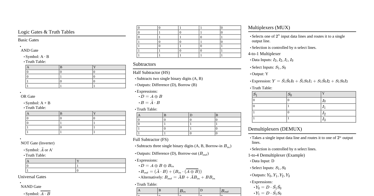
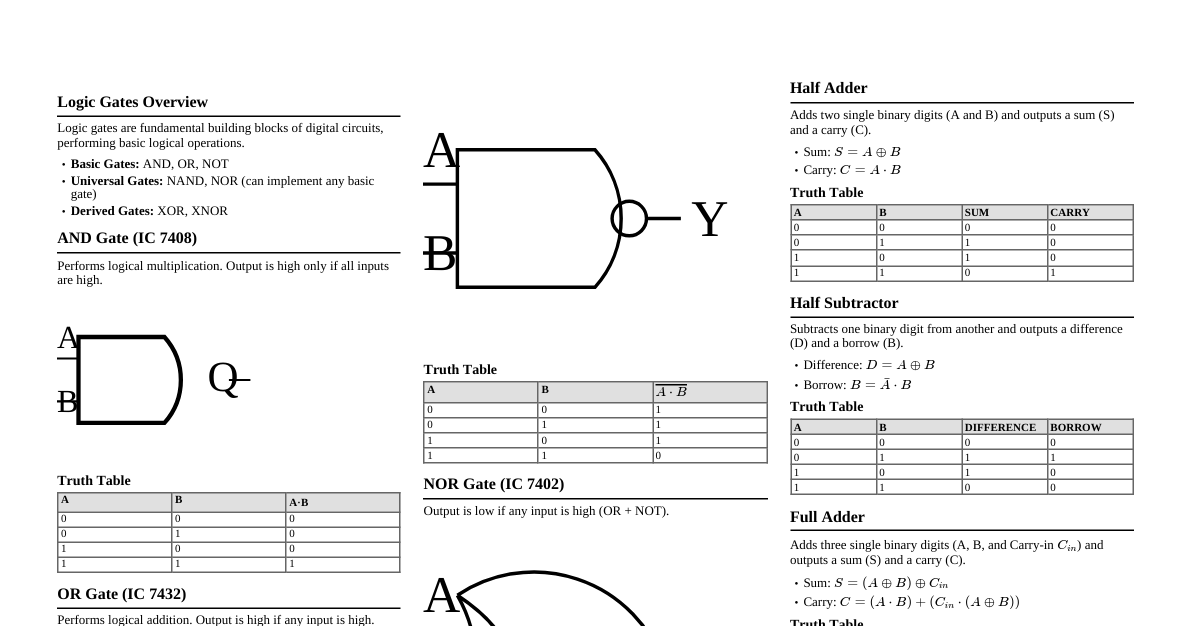
Number Systems & Conversions Binary, Octal, Decimal, Hexadecimal Binary (Base 2): Uses 0 and 1. Octal (Base 8): Uses 0-7. Decimal (Base 10): Uses 0-9. Hexadecimal (Base 16): Uses 0-9, A-F (A=10, F=15). Conversions Decimal to Binary: Repeated division by 2, collect remainders. Binary to Decimal: Sum of (digit $\times 2^{\text{position}}$). Decimal to Octal/Hex: Similar repeated division by 8 or 16. Binary to Octal: Group binary digits in 3s from right. Binary to Hexadecimal: Group binary digits in 4s from right. Octal/Hex to Binary: Convert each digit to its 3/4-bit binary equivalent. Complements 1's Complement: Invert all bits (0 to 1, 1 to 0). 2's Complement: 1's complement + 1. Used for representing negative numbers and subtraction in binary. Signed Number Representation Signed Magnitude: MSB (Most Significant Bit) for sign (0=positive, 1=negative), rest for magnitude. 1's Complement: Invert positive number bits for negative. 2's Complement: 2's complement of positive number for negative. Most common due to unique zero and simpler arithmetic. Binary Arithmetic Addition $0+0=0$ $0+1=1$ $1+0=1$ $1+1=0$ (carry 1) Subtraction (using 2's complement) Find 2's complement of the subtrahend. Add it to the minuend. If there's a carry-out, discard it (result is positive). If no carry-out, the result is negative and in 2's complement form (take 2's complement to get magnitude). Logic Gates NOT Gate (Inverter): $Y = \bar{A}$ A Y 0 1 1 0 AND Gate: $Y = A \cdot B$ A B Y 0 0 0 0 1 0 1 0 0 1 1 1 OR Gate: $Y = A + B$ A B Y 0 0 0 0 1 1 1 0 1 1 1 1 NAND Gate: $Y = \overline{A \cdot B}$ (NOT AND) A B Y 0 0 1 0 1 1 1 0 1 1 1 0 NOR Gate: $Y = \overline{A + B}$ (NOT OR) A B Y 0 0 1 0 1 0 1 0 0 1 1 0 XOR Gate (Exclusive OR): $Y = A \oplus B = \bar{A}B + A\bar{B}$ A B Y 0 0 0 0 1 1 1 0 1 1 1 0 XNOR Gate (Exclusive NOR): $Y = \overline{A \oplus B} = AB + \bar{A}\bar{B}$ A B Y 0 0 1 0 1 0 1 0 0 1 1 1 Combinational Logic Circuits Half Adder Adds two single binary digits (A, B). Outputs: Sum (S) and Carry (C). $S = A \oplus B$ $C = A \cdot B$ Full Adder Adds three single binary digits (A, B, Carry-in $C_{in}$). Outputs: Sum (S) and Carry-out ($C_{out}$). $S = A \oplus B \oplus C_{in}$ $C_{out} = AB + BC_{in} + AC_{in}$ Sequential Logic Circuits (Flip-Flops) Memory elements, store 1 bit of information. Output depends on current inputs and past output (state). Triggered by clock signals (edge-triggered or level-triggered). S-R Flip-Flop (Set-Reset) Inputs: S (Set), R (Reset). Outputs: Q, $\bar{Q}$. NOR gate based: Active LOW inputs. S R Q$_{next}$ $\bar{Q}_{next}$ State 0 0 Q $\bar{Q}$ No Change 0 1 0 1 Reset 1 0 1 0 Set 1 1 ? ? Forbidden (Invalid) NAND gate based: Active HIGH inputs. S R Q$_{next}$ $\bar{Q}_{next}$ State 0 0 ? ? Forbidden (Invalid) 0 1 1 0 Set 1 0 0 1 Reset 1 1 Q $\bar{Q}$ No Change Clocked S-R Flip-Flop: Has a clock input. State changes only on clock edge/level. Race-around condition: In level-triggered S-R, if S=R=1 and clock is high, output oscillates. D Flip-Flop (Data) Inputs: D (Data). Outputs: Q, $\bar{Q}$. $Q_{next} = D$ (Output follows input D on clock edge). Eliminates the forbidden state of S-R flip-flop. Used for storing data. J-K Flip-Flop Inputs: J, K. Outputs: Q, $\bar{Q}$. No forbidden state. Handles $J=K=1$ by toggling the output. Truth Table: (for positive edge-triggered) J K Q$_{next}$ State 0 0 Q No Change 0 1 0 Reset 1 0 1 Set 1 1 $\bar{Q}$ Toggle Master-Slave J-K Flip-Flop: Used to overcome race-around condition in level-triggered J-K. T Flip-Flop (Toggle) Inputs: T (Toggle). Outputs: Q, $\bar{Q}$. $Q_{next} = \bar{Q}$ when T=1 (toggles). $Q_{next} = Q$ when T=0 (no change). Can be made from a J-K flip-flop by connecting J and K inputs together to T. Semiconductors & Diodes Intrinsic Semiconductors Pure semiconductors (e.g., Silicon, Germanium). Conductivity increases with temperature. Number of electrons equals number of holes ($n_i = p_i$). Extrinsic Semiconductors (Doping) Adding impurities to intrinsic semiconductors to increase conductivity. N-type: Doped with pentavalent impurities (e.g., Phosphorus, Arsenic). Majority carriers: Electrons. Minority carriers: Holes. Donor impurities. P-type: Doped with trivalent impurities (e.g., Boron, Gallium). Majority carriers: Holes. Minority carriers: Electrons. Acceptor impurities. P-N Junction Diode Formed by joining P-type and N-type semiconductors. Depletion Region: Region near the junction devoid of free charge carriers. Formed due to diffusion of electrons from N to P and holes from P to N, creating an electric field. Barrier Potential: Voltage developed across the depletion region due to the electric field (e.g., $\approx 0.7V$ for Si, $\approx 0.3V$ for Ge). Diode Biasing Forward Bias: P-side connected to positive terminal of battery, N-side to negative. Reduces depletion region width. Reduces barrier potential. Allows current flow (majority carriers). Diode acts like a closed switch. Reverse Bias: P-side connected to negative terminal, N-side to positive. Increases depletion region width. Increases barrier potential. Very small current flows (minority carriers - leakage current). Diode acts like an open switch. V-I Characteristics of a Diode Forward Characteristics: Current is very small until the knee voltage (barrier potential) is reached. After knee voltage, current increases exponentially with voltage. Reverse Characteristics: Very small reverse saturation current flows. At a certain reverse voltage (breakdown voltage), current increases sharply due to avalanche or Zener breakdown. Diode Equation $I = I_0 (e^{V/\eta V_T} - 1)$ $I$: Diode current $I_0$: Reverse saturation current $V$: Voltage across diode $\eta$: Ideality factor ($\approx 1$ for Ge, $\approx 2$ for Si) $V_T$: Thermal voltage ($kT/q \approx 26mV$ at room temp) Bipolar Junction Transistors (BJTs) Three-terminal semiconductor device used for amplification or switching. Consists of two P-N junctions. Terminals: Emitter (E), Base (B), Collector (C). Types of BJTs NPN Transistor: N-type Emitter, P-type Base, N-type Collector. PNP Transistor: P-type Emitter, N-type Base, P-type Collector. Symbol for NPN: Arrow on emitter points out. Symbol for PNP: Arrow on emitter points in. Transistor Regions Emitter: Heavily doped, emits majority carriers. Base: Lightly doped and very thin, allows most carriers to pass to collector. Collector: Moderately doped, collects carriers from base. Larger area for heat dissipation. BJT Biasing (for Active Region Operation - Amplification) Emitter-Base Junction: Always forward-biased. Collector-Base Junction: Always reverse-biased. Example: NPN in active region: Base positive w.r.t. Emitter (V$_{BE}$ > 0.7V), Collector positive w.r.t. Base (V$_{CB}$ positive). Transistor Currents Emitter current ($I_E$) is the sum of Collector current ($I_C$) and Base current ($I_B$). $I_E = I_C + I_B$ Current gain: $\alpha = I_C / I_E$ (typically 0.95 - 0.99) $\beta = I_C / I_B$ (typically 50 - 200) Relationship: $\beta = \alpha / (1 - \alpha)$ and $\alpha = \beta / (1 + \beta)$ Operating Regions of BJT Active Region: E-B forward, C-B reverse. Used for amplification. Saturation Region: E-B forward, C-B forward. Transistor acts as a closed switch. Cut-off Region: E-B reverse, C-B reverse. Transistor acts as an open switch. Reverse Active Region: E-B reverse, C-B forward. Rarely used. Common Configurations Common Emitter (CE): Input to Base, Output from Collector, Emitter common. High current and voltage gain. Phase inversion (180 degrees). Most common for amplification. Common Base (CB): Input to Emitter, Output from Collector, Base common. High voltage gain, current gain No phase inversion. Good for high-frequency applications. Common Collector (CC) / Emitter Follower: Input to Base, Output from Emitter, Collector common. High current gain, voltage gain No phase inversion. Used for impedance matching.