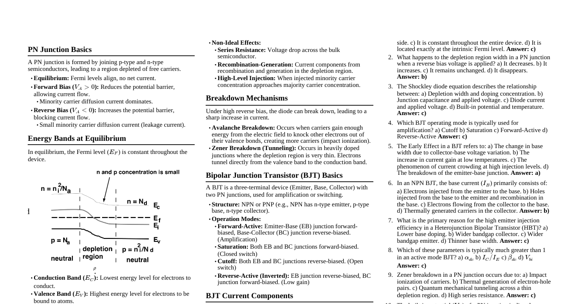
ETCE Electronics Cheatsheet
Cheatsheet Content
Unit 1: Diodes and Their Applications 1. Half Wave and Full Wave Rectifier Half Wave Rectifier (HWR): Converts AC to pulsating DC. Only half cycle of AC passes. Circuit: Diode, transformer, load resistor. Working: During positive half cycle, diode is forward biased and conducts. During negative half cycle, diode is reverse biased and blocks current. Output: Pulsating DC. Full Wave Rectifier (FWR): Converts both halves of AC to pulsating DC. Types: Center-Tapped FWR: Uses two diodes and a center-tapped transformer. Bridge FWR: Uses four diodes in a bridge configuration, no center-tapped transformer needed. Working (Bridge FWR): During positive half cycle, D1 & D2 conduct. During negative half cycle, D3 & D4 conduct. Current through load always in same direction. Output: More continuous pulsating DC than HWR. Diagrams: (Imagine standard HWR/FWR circuit diagrams with input/output waveforms) HWR Circuit (conceptual) AC In RL FWR Bridge Circuit (conceptual) AC In RL 2. RMS Voltage, Average Voltage, Efficiency of FWR RMS Voltage ($V_{rms}$): Effective value of AC voltage, $V_{rms} = \frac{V_m}{\sqrt{2}}$ (sine wave). Average Voltage ($V_{avg}$): DC component of the rectified output. HWR: $V_{avg} = \frac{V_m}{\pi}$ FWR: $V_{avg} = \frac{2V_m}{\pi}$ Efficiency ($\eta$): Ratio of DC output power to AC input power. HWR: $\eta = 40.6\%$ FWR: $\eta = 81.2\%$ 3. Zener Diode as Voltage Regulator Zener Diode: A specially doped diode designed to operate in reverse breakdown region without damage. Maintains a constant voltage across its terminals despite changes in current or input voltage. Working: When reverse biased, if voltage reaches Zener voltage ($V_Z$), it breaks down and conducts heavily, maintaining $V_Z$ across it. Connected in parallel with the load. A series resistor ($R_S$) limits the current through the Zener. Regulation: Line Regulation: If input voltage changes, Zener current changes to keep $V_Z$ constant. Load Regulation: If load current changes, Zener current adjusts to keep $V_Z$ constant. Diagram: (Imagine Zener regulator circuit with series resistor and parallel load) Zener Regulator (conceptual) Vin Rs Zener RL 4. Capacitor, Inductor, and Pi filters Filters are used to smooth the pulsating DC output of rectifiers, reducing ripple voltage. Capacitor Filter: (Shunt capacitor) Connected in parallel with the load. Charges during positive peak, discharges through load when diode is reverse biased. Reduces ripple by storing energy. Ripple voltage inversely proportional to capacitance and load resistance. Inductor Filter: (Series inductor) Connected in series with the load. Opposes changes in current (due to its inductance), thus smoothing the output current. Effective for heavy loads (low $R_L$). LC Filter (L-section): Combination of series inductor and shunt capacitor. Provides better filtering than individual components. Inductor smooths current, capacitor smooths voltage. Pi Filter ($\pi$-section): Consists of a shunt capacitor at input, a series inductor, and another shunt capacitor at output. Provides excellent ripple reduction. First capacitor reduces input ripple, inductor smooths current, second capacitor further smooths voltage. Often used in power supplies requiring very low ripple. Diagrams: (Conceptual diagrams for C, L, LC, and Pi filters) Capacitor Filter (conceptual) C Rect. Out RL Pi Filter (conceptual) C1 L C2 Rect. Out RL 5. Zener vs. Avalanche Breakdown Feature Zener Breakdown Avalanche Breakdown Mechanism Strong electric field causes direct rupture of covalent bonds, freeing charge carriers. High reverse voltage accelerates minority carriers which collide with atoms, creating new electron-hole pairs (impact ionization). Doping Heavily doped p-n junction. Lightly doped p-n junction. Junction Width Narrow depletion region. Wider depletion region. Breakdown Voltage Typically occurs below 5V. Typically occurs above 5V. Temperature Coeff. Negative (breakdown voltage decreases with increasing temperature). Positive (breakdown voltage increases with increasing temperature). Application Voltage regulation (low voltage). Voltage regulation (high voltage), surge protection. 6. Varactor and Schottky Diodes Varactor Diode (Variable Capacitance Diode): Principle: A reverse-biased p-n junction exhibits capacitance, which depends on the applied reverse voltage. $C_T = \frac{\epsilon A}{W_d}$, where $W_d$ is depletion width. Working: As reverse voltage increases, depletion width ($W_d$) increases, causing capacitance ($C_T$) to decrease. Applications: Voltage-controlled oscillators (VCOs), frequency multipliers, tuning circuits in radios/TVs. Schottky Diode (Hot Carrier Diode): Principle: Formed by a metal-semiconductor junction (e.g., aluminum-n-type silicon). Working: Electrons from semiconductor enter metal as "hot carriers." No depletion region formed by p-n junction. Characteristics: Very fast switching speed (due to absence of minority carrier storage effects), lower forward voltage drop ($0.15V - 0.45V$). Applications: High-frequency rectifiers, switching power supplies, RF applications, clamp diodes. Diagrams: (Symbols for Varactor and Schottky diodes) Varactor Diode Symbol Schottky Diode Symbol 7. Clipper and Clamper Circuits Clipper Circuits (Limiters): Function: Remove (clip) a portion of the input signal above or below a certain reference voltage level. Types: Series Clipper: Diode is in series with the load. Parallel Clipper: Diode is in parallel with the load. Positive Clipper: Clips positive half cycle. Negative Clipper: Clips negative half cycle. Biased Clipper: Clips at a specific DC level using a reference voltage. Applications: Wave shaping, protection circuits, amplitude limiting. Clamper Circuits (DC Restorers): Function: Shift the entire AC input signal up or down to a different DC level without altering the waveform shape. Components: Capacitor, diode, and a resistor (for discharge path). Working: Capacitor charges to the peak voltage, and the diode ensures that the capacitor discharges only through the resistor, thus shifting the DC level. Types: Positive clamper, negative clamper, biased clamper. Applications: TV receivers (sync pulse restoration), DC restoration in communication systems. Diagrams: (Conceptual examples of a simple positive parallel clipper and a positive clamper) Positive Parallel Clipper (conceptual) Vin RL Positive Clamper (conceptual) C Vin RL 8. Transformer Utilization Factor (TUF) Definition: TUF is a measure of how effectively a transformer is utilized in a rectifier circuit. It is the ratio of DC power delivered to the load to the AC VA rating of the transformer secondary. $$ TUF = \frac{P_{dc}}{VA_{ac (secondary)}} $$ Importance: Indicates transformer efficiency in delivering power. A higher TUF means better utilization of the transformer's capacity. Helps in selecting the appropriate transformer for a given rectifier application to avoid oversizing or undersizing. Calculation for Full Wave Rectifier (FWR): For center-tapped FWR: Each half of the secondary winding carries current only for half the cycle. $$ P_{dc} = V_{dc} I_{dc} = \frac{2V_m}{\pi} \frac{2I_m}{\pi} R_L = \frac{4V_m I_m}{\pi^2} R_L $$ $$ VA_{ac (secondary)} = V_{rms} I_{rms} \times 2 (\text{for each half winding}) = \frac{V_m}{\sqrt{2}} \frac{I_m}{\sqrt{2}} \times 2 = V_m I_m $$ $$ TUF_{FWR (center-tapped)} = \frac{4V_m I_m / \pi^2}{V_m I_m} = \frac{4}{\pi^2} \approx 0.406 $$ This value implies that the transformer is poorly utilized, with only about 40.6% of its VA rating being used for DC power delivery. For Bridge FWR: Both windings are used for the full cycle. $$ TUF_{FWR (bridge)} \approx 0.812 $$ The bridge rectifier has a higher TUF because the transformer secondary is utilized for the full cycle. 9. Compare Bridge and Centre-Tapped Full Wave Rectifiers Feature Center-Tapped FWR Bridge FWR Transformer Requires center-tapped transformer (more expensive, larger). Does not require center-tapped transformer (standard transformer, cheaper). Number of Diodes Two diodes. Four diodes. Peak Inverse Voltage (PIV) $2V_m$ (higher). Diodes must withstand higher reverse voltage. $V_m$ (lower). Diodes can have lower reverse voltage rating. DC Output Voltage Same as Bridge FWR ($2V_m/\pi$). Same as Center-Tapped FWR ($2V_m/\pi$). Transformer Utilization Factor (TUF) Lower ($\approx 0.406$). Higher ($\approx 0.812$). Better utilization. Current through Diodes Each diode conducts for half a cycle. Two diodes conduct simultaneously for each half cycle. Efficiency $81.2\%$. $81.2\%$. Cost/Complexity Simpler circuit, but expensive transformer. More complex circuit (4 diodes), but cheaper transformer. 10. Filter Circuits in DC Power Supply Design Need for Filters: Rectifiers convert AC to pulsating DC, which contains significant AC components (ripple). Electronic circuits require a smooth, constant DC voltage for stable and reliable operation. Ripple voltage can cause hum in audio circuits, instability in digital circuits, and errors in measurement systems. Filters are essential to reduce this ripple to an acceptable level. Role of Filters: Capacitor Filters: Act as energy storage devices. They charge during the peaks of the rectified voltage and discharge through the load when the rectifier output falls, thus maintaining a relatively constant output voltage. They are effective for light loads. Inductor Filters: Act as current smoothers. Inductors oppose changes in current, so they smooth out the pulsating current from the rectifier, leading to a more constant output current. They are effective for heavy loads. LC Filters (L-section, $\pi$-section): Combine the advantages of both capacitors and inductors. L-section provides better smoothing than individual C or L. $\pi$-section (CLC filter) offers superior ripple reduction and is widely used for applications requiring very low ripple. The input capacitor handles initial ripple, the inductor smooths current, and the output capacitor further smooths voltage. Design Considerations: Ripple Factor: A measure of ripple content; filters aim to minimize this. Load Current: Type of filter depends on the expected load current (e.g., C filter for light loads, L or LC for heavy loads). Cost and Size: Larger capacitors and inductors provide better filtering but are more expensive and bulky. Voltage Regulation: Filters can impact voltage regulation; sometimes active regulators are used after filters. Unit 2: Bipolar Junction Transistor and Its Biasing 1. Construction and Working of CB, CE, and CC Transistor Configurations A BJT has three terminals: Emitter (E), Base (B), Collector (C). It has three configurations based on which terminal is common to input and output. Common Base (CB) Configuration: Input: Emitter-Base junction. Output: Collector-Base junction. Base is common. Characteristics: High voltage gain, very low input impedance, very high output impedance. Current gain ($\alpha = I_C/I_E$) is always less than 1 (typically 0.95 to 0.99). Applications: High-frequency applications, impedance matching. Common Emitter (CE) Configuration: Input: Base-Emitter junction. Output: Collector-Emitter junction. Emitter is common. Characteristics: High current gain ($\beta = I_C/I_B$), high voltage gain, medium input and output impedance. Provides phase inversion (180°). Most widely used configuration for amplification. Applications: General purpose amplifiers, switching circuits. Common Collector (CC) Configuration (Emitter Follower): Input: Base-Collector junction. Output: Emitter-Collector junction. Collector is common. Characteristics: High current gain ($\beta+1$), voltage gain close to 1 (unity), high input impedance, low output impedance. No phase inversion. Applications: Impedance matching, buffer stages. Working Principle (NPN Transistor): Forward Bias Emitter-Base: Minority carriers (electrons for NPN) from emitter are injected into the base. Reverse Bias Collector-Base: Most electrons from base diffuse into the collector due to the strong electric field, creating collector current $I_C$. A small recombination occurs in the base, forming base current $I_B$. $I_E = I_B + I_C$. Diagrams: (Symbols for NPN/PNP transistors and basic circuit diagrams for CB, CE, CC configurations) NPN Transistor Symbol C B E PNP Transistor Symbol C B E 2. Relation between Alpha ($\alpha$) and Beta ($\beta$) These are the current gain parameters for a BJT. Alpha ($\alpha$): Current gain in Common Base (CB) configuration. $$ \alpha = \frac{I_C}{I_E} $$ ($I_C$ = collector current, $I_E$ = emitter current). $\alpha$ is typically between 0.95 and 0.99. Beta ($\beta$): Current gain in Common Emitter (CE) configuration. Also called $h_{FE}$. $$ \beta = \frac{I_C}{I_B} $$ ($I_B$ = base current). $\beta$ is typically between 50 and 300. Relationship: We know $I_E = I_B + I_C$. To find $\alpha$ in terms of $\beta$: $$ I_E = I_B + I_C = \frac{I_C}{\beta} + I_C = I_C \left( \frac{1}{\beta} + 1 \right) = I_C \frac{1+\beta}{\beta} $$ $$ \alpha = \frac{I_C}{I_E} = \frac{I_C}{I_C \frac{1+\beta}{\beta}} = \frac{\beta}{1+\beta} $$ To find $\beta$ in terms of $\alpha$: $$ \alpha = \frac{\beta}{1+\beta} \Rightarrow \alpha(1+\beta) = \beta \Rightarrow \alpha + \alpha\beta = \beta $$ $$ \alpha = \beta - \alpha\beta = \beta(1-\alpha) $$ $$ \beta = \frac{\alpha}{1-\alpha} $$ 3. DC Load Line and its Significance in Transistor Biasing DC Load Line: A straight line drawn on the output characteristics ($I_C$ vs $V_{CE}$) of a transistor. It represents all possible DC operating points (Q-points) for a given circuit configuration. Equation: For a common emitter configuration with collector resistor $R_C$ and supply voltage $V_{CC}$: $$ V_{CE} = V_{CC} - I_C R_C $$ Y-intercept: When $V_{CE} = 0$, $I_C = \frac{V_{CC}}{R_C}$. X-intercept: When $I_C = 0$, $V_{CE} = V_{CC}$. Significance: Determining Q-point: The intersection of the DC load line with the transistor's output characteristics (for a specific $I_B$) defines the Q-point (Quiescent Operating Point). Operating Region: Helps visualize where the transistor is operating (active, saturation, or cutoff regions). The Q-point should ideally be in the center of the active region for undistorted amplification. Maximum Swing: Helps determine the maximum possible undistorted output voltage and current swing. Biasing Design: Essential tool for designing biasing circuits to set a stable Q-point, ensuring the transistor operates correctly under varying conditions (temperature, $\beta$ variations). Diagram: (Conceptual output characteristics with DC load line and Q-point) DC Load Line (conceptual) IC VCE Vcc/Rc Vcc Q Saturation Cutoff 4. Define Q-point and explain its importance Q-point (Quiescent Operating Point / Quiescent Point): The DC operating point of a transistor, defined by the values of collector current ($I_C$) and collector-emitter voltage ($V_{CE}$) when no AC signal is applied. It represents the steady-state DC voltage and current conditions of the transistor. Importance: Undistorted Amplification: For a transistor to amplify an AC signal without distortion, its Q-point must be set in the active region, preferably near the center of the DC load line. This allows for maximum positive and negative swings of the output signal without hitting saturation or cutoff. Bias Stability: The Q-point should be stable and independent of variations in temperature, transistor parameters (like $\beta$), and power supply fluctuations. Unstable Q-point leads to distortion or thermal runaway. Power Dissipation: The Q-point determines the DC power dissipated by the transistor ($P_D = V_{CE} I_C$), which must be within the transistor's safe operating area (SOA). Efficiency: For power amplifiers, the Q-point directly influences the amplifier's class of operation (Class A, B, AB, C) and thus its efficiency. Design Basis: Biasing circuits are designed specifically to establish and maintain a stable Q-point. 5. Differentiate between Biasing Methods Biasing refers to setting the DC operating point (Q-point) of a transistor. Different methods offer varying degrees of stability. Method Description Advantages Disadvantages Base Bias (Fixed Bias) Single resistor $R_B$ connected from $V_{CC}$ to base. Simple circuit, few components. Highly unstable Q-point (very sensitive to $\beta$ and temperature variations). Prone to thermal runaway. Collector Feedback Bias Resistor $R_B$ connected from collector to base. Improved stability over fixed bias (negative feedback). Q-point is more stable against $\beta$ variations. Still sensitive to temperature. Reduces voltage gain due to feedback. Emitter Feedback Bias (Self-Bias) Resistor $R_E$ connected in the emitter path, with $R_B$ from $V_{CC}$ to base. Good stability against $\beta$ and temperature variations due to emitter feedback. Requires two power supplies (or a capacitor at $R_E$ for AC). Input impedance is reduced. Voltage Divider Bias (Potential Divider Bias) Two resistors ($R_1, R_2$) form a voltage divider at the base. Emitter resistor $R_E$ also present. Most stable biasing method. Q-point is almost independent of $\beta$ and temperature. More components, slightly increased current drain from supply. 6. Derivation for Stability Factor ($S$) and its Role in Biasing Stability Factor ($S$): A measure of how much the Q-point (specifically $I_C$) changes with respect to variations in collector leakage current ($I_{CO}$), $\beta$, or $V_{BE}$. $$ S = \frac{\partial I_C}{\partial I_{CO}} $$ An ideal stability factor is 1, meaning $I_C$ is independent of $I_{CO}$. A higher value of $S$ indicates poor stability. Derivation for Voltage Divider Bias: Approximate analysis (assuming $R_B = R_1 || R_2$ and $V_{TH} = V_{CC} \frac{R_2}{R_1+R_2}$): Applying KVL to Base-Emitter loop: $$ V_{TH} - I_B R_B - V_{BE} - I_E R_E = 0 $$ $$ V_{TH} - I_B R_B - V_{BE} - (I_C + I_B) R_E = 0 $$ Using $I_C \approx \beta I_B$, so $I_B = I_C/\beta$: $$ V_{TH} - \frac{I_C}{\beta} R_B - V_{BE} - (I_C + \frac{I_C}{\beta}) R_E = 0 $$ $$ V_{TH} - V_{BE} = I_C \left( \frac{R_B}{\beta} + R_E + \frac{R_E}{\beta} \right) $$ $$ I_C = \frac{V_{TH} - V_{BE}}{R_E + (R_B + R_E)/\beta} $$ The stability factor for $I_{CO}$ is given by: $$ S = \frac{1+R_B/R_E}{1+\frac{R_B}{R_E} \frac{1}{1+\beta}} \approx 1 + \frac{R_B}{R_E} $$ where $R_B = R_1 || R_2$. To achieve good stability (low $S$), $R_B$ should be much smaller than $R_E$. This means the voltage divider current should be much larger than the base current. Role in Biasing: Minimizing Variation: A low stability factor ensures that the Q-point ($I_C, V_{CE}$) remains relatively constant despite changes in temperature (which affects $I_{CO}$ and $V_{BE}$) and variations in $\beta$ from one transistor to another. Preventing Thermal Runaway: If $I_C$ increases due to temperature, power dissipation increases, further increasing temperature, leading to further $I_C$ increase. A low stability factor helps prevent this positive feedback loop. Reliable Operation: Proper biasing with a low $S$ is crucial for reliable and predictable amplifier operation, especially in mass production where $\beta$ values can vary significantly. 7. Thermal Runaway and its Prevention Thermal Runaway: A destructive positive feedback process in a BJT where an increase in collector current ($I_C$) leads to an increase in junction temperature, which in turn causes a further increase in $I_C$, eventually leading to device destruction. Mechanism: Temperature increases (due to ambient temp or power dissipation). $I_{CO}$ (reverse leakage current) increases significantly with temperature. Increased $I_{CO}$ causes $I_C$ to increase ($I_C = \beta I_B + (1+\beta)I_{CO}$). Increased $I_C$ leads to increased power dissipation ($P_D = V_{CE} I_C$) in the transistor. Increased power dissipation further increases the junction temperature, completing the positive feedback loop. Prevention Methods: Biasing with Emitter Feedback (Voltage Divider Bias): This is the most effective method. The emitter resistor ($R_E$) provides negative feedback. If $I_C$ increases, $V_E = I_E R_E$ increases, which reduces $V_{BE}$ (if $V_B$ is fixed by a voltage divider). A reduced $V_{BE}$ reduces $I_B$, which in turn reduces $I_C$, counteracting the initial increase. Heat Sinks: Mechanical devices that dissipate heat away from the transistor package to the ambient air, keeping the junction temperature within limits. Thermistor/Diode Compensation: Thermistor: A resistor with a negative temperature coefficient (resistance decreases with increasing temperature). Can be used in the base biasing circuit to reduce $I_B$ as temperature rises. Diode: A diode in series with the base resistor can be forward-biased. Its $V_F$ decreases with temperature, which can be designed to compensate for the decrease in $V_{BE}$ of the transistor, thus stabilizing $I_C$. Low Stability Factor ($S$): Designing the biasing circuit to have a low stability factor is crucial. For voltage divider bias, ensure $R_B/R_E$ is small. Selecting Transistors with Low $I_{CO}$: Using transistors with inherently low leakage currents. Operating within SOA: Ensuring the transistor operates within its Safe Operating Area, considering maximum power dissipation, voltage, and current ratings. 8. Compare CB, CE, and CC Configurations in Terms of Input and Output Impedance, Gain, and Phase Shift Parameter Common Base (CB) Common Emitter (CE) Common Collector (CC) Input Impedance ($Z_{in}$) Very Low (tens of ohms) Medium (few k$\Omega$) Very High (tens to hundreds of k$\Omega$) Output Impedance ($Z_{out}$) Very High (hundreds of k$\Omega$ to M$\Omega$) Medium (few k$\Omega$) Very Low (tens to hundreds of ohms) Current Gain ($A_i$) Low ($\alpha High ($\beta$) High ($\beta+1$) Voltage Gain ($A_v$) High (typically 100-500) High (typically 50-500) Approximately 1 (unity) Power Gain ($A_p$) Medium Very High Medium Phase Shift (Input vs Output) 0° (No phase inversion) 180° (Phase inversion) 0° (No phase inversion) Applications High-frequency amplifiers, impedance matching (low Z_in source to high Z_out load). General purpose voltage amplification, switching. Buffer, impedance matching (high Z_in source to low Z_out load), current driver. Unit 3: Small Signal Transistor Amplifiers 1. Hybrid Parameter Model for CE Amplifier The hybrid parameter (h-parameter) model is a two-port network representation used to analyze the small-signal behavior of transistors, especially at low frequencies. Definition: The h-parameters relate input voltage $V_1$, output current $I_2$ to input current $I_1$ and output voltage $V_2$. $$ V_1 = h_{11} I_1 + h_{12} V_2 $$ $$ I_2 = h_{21} I_1 + h_{22} V_2 $$ For CE configuration, the parameters are: $V_{be} = h_{ie} I_b + h_{re} V_{ce}$ $I_c = h_{fe} I_b + h_{oe} V_{ce}$ h-parameters for CE: $h_{ie}$ (input impedance with output shorted): $h_{ie} = (\frac{V_{be}}{I_b})_{V_{ce}=0}$ (ohms) $h_{re}$ (reverse voltage ratio with input open): $h_{re} = (\frac{V_{be}}{V_{ce}})_{I_b=0}$ (dimensionless) $h_{fe}$ (forward current gain with output shorted): $h_{fe} = (\frac{I_c}{I_b})_{V_{ce}=0}$ (dimensionless, equivalent to $\beta$) $h_{oe}$ (output admittance with input open): $h_{oe} = (\frac{I_c}{V_{ce}})_{I_b=0}$ (siemens) Equivalent Circuit: The h-parameter model represents the transistor as a voltage source $h_{re}V_{ce}$ in the input loop and a current source $h_{fe}I_b$ in the output loop. Diagram: (h-parameter equivalent circuit for CE configuration) CE h-Parameter Model (conceptual) hie + - Ib hreVce hfeIb hoe Ic Vce 2. Expressions for Current Gain, Voltage Gain, Input Impedance, and Output Impedance using h-parameters For a CE amplifier with a load resistor $R_L$ connected at the output. Current Gain ($A_i$): $$ A_i = \frac{I_c}{I_b} = \frac{h_{fe}}{1 + h_{oe} R_L} $$ If $h_{oe} R_L \ll 1$, then $A_i \approx h_{fe}$. Voltage Gain ($A_v$): $$ A_v = \frac{V_{ce}}{V_{be}} = \frac{-h_{fe} R_L}{h_{ie} + (h_{ie} h_{oe} - h_{fe} h_{re}) R_L} $$ If $h_{re}$ and $h_{oe}$ are very small (often assumed for simplification), then: $$ A_v \approx \frac{-h_{fe} R_L}{h_{ie}} $$ The negative sign indicates 180° phase shift. Input Impedance ($Z_{in}$): $$ Z_{in} = \frac{V_{be}}{I_b} = h_{ie} - \frac{h_{fe} h_{re} R_L}{1 + h_{oe} R_L} $$ If $h_{re}$ and $h_{oe}$ are very small: $$ Z_{in} \approx h_{ie} $$ Output Impedance ($Z_{out}$): $$ Z_{out} = (\frac{V_{ce}}{I_c})_{V_s=0} = \frac{1}{h_{oe} - \frac{h_{fe} h_{re}}{h_{ie} + R_S}} $$ where $R_S$ is the source resistance. If $h_{re}$ and $h_{oe}$ are very small: $$ Z_{out} \approx \frac{1}{h_{oe}} $$ 3. RC Coupled Amplifier and its Frequency Response Curve RC Coupled Amplifier: A multi-stage amplifier where the output of one stage is connected to the input of the next stage using a coupling capacitor (C) and a biasing resistor (R). Operation: The coupling capacitor blocks DC, ensuring that the DC bias of one stage does not affect the next. It passes the AC signal, allowing amplification across stages. Resistors are used for biasing and as load resistors. Advantages: Good frequency response, low cost, small size. Disadvantages: Impedance mismatching, gain decreases at low and high frequencies. Frequency Response Curve: A graph of voltage gain (dB) vs. frequency (log scale). Mid-frequency Range: Gain is constant and maximum. Coupling and bypass capacitors act as short circuits, and internal transistor capacitances are negligible. Low-frequency Range: Gain decreases. Coupling capacitors ($C_C$) and emitter bypass capacitors ($C_E$) start to have significant impedance, reducing the signal reaching the base and increasing negative feedback (if $C_E$ is not effective). High-frequency Range: Gain decreases. Internal transistor junction capacitances ($C_{be}, C_{bc}$) start to act as shunts, reducing the effective load resistance and bypassing the signal. Diagram: (Conceptual RC coupled amplifier stage and its frequency response) RC Coupled Stage (conceptual) C_in R1 R2 C E B Rc Vcc C_c V_out Frequency Response (conceptual) Gain (dB) Frequency (log) fL fH Mid-band Gain 4. Direct Coupled Amplifier and its Advantages/Disadvantages Direct Coupled Amplifier: A multi-stage amplifier where the output of one stage is directly connected to the input of the next stage without any coupling components (capacitors or transformers). Operation: The output DC voltage of one stage serves as the input DC bias for the next stage. This means that the DC levels are directly transferred between stages, which makes biasing more complex. Advantages: Excellent Low-Frequency Response: No coupling capacitors means no roll-off at low frequencies (down to DC). Ideal for amplifying DC signals or very slow-changing signals. Simplicity: Fewer components (no coupling capacitors), leading to simpler circuit design. Cost-Effective: Reduced component count means lower cost. Can be Integrated: Easier to implement in integrated circuits (ICs). Disadvantages: DC Drift/Offset Problems: Small changes in DC bias of the first stage (due to temperature variation, transistor parameter changes) are amplified by subsequent stages, leading to significant output DC offset, which can saturate the output. Complex Biasing: Each stage's DC output voltage must be compatible with the next stage's input bias requirements, making biasing design challenging. Poor Temperature Stability: Highly susceptible to thermal runaway due to direct coupling of DC levels. Limited Gain: Often limited to a few stages to control DC drift. Applications: Operational amplifiers (Op-Amps), differential amplifiers, instrumentation amplifiers, whenever DC or very low-frequency amplification is required. 5. Transformer Coupled Amplifier and its Application in Power Stages Transformer Coupled Amplifier: A multi-stage amplifier where the output of one stage is coupled to the input of the next stage (or to the load) using a transformer. Operation: The primary winding of the transformer acts as the collector load. The secondary winding is connected to the next stage or load. The transformer blocks DC but passes AC. Advantages: Excellent Impedance Matching: Transformers can step up or step down impedance ($Z_1/Z_2 = (N_1/N_2)^2$), allowing for efficient power transfer from a high-output impedance stage to a low-load impedance (e.g., speaker). This is crucial for power amplifiers. High Voltage Gain: Can provide voltage step-up (if $N_{secondary} > N_{primary}$). DC Isolation: Provides DC isolation between stages, preventing DC bias interference. Improved Efficiency: Better efficiency than RC coupled amplifiers in power stages due to reduced DC power loss in load resistance. Disadvantages: Poor Frequency Response: Low frequency roll-off due to the transformer's primary inductance. High frequency roll-off due to leakage inductance and stray capacitance of the transformer windings. Bulky and Expensive: Transformers are large, heavy, and costly, especially for audio frequencies. Distortion: Non-linear magnetizing characteristics of the transformer core can introduce distortion. Application in Power Stages: Transformer coupling is predominantly used in the output (power) stages of audio amplifiers (Class A, B, AB) to achieve efficient power transfer to low impedance loads like loudspeakers (typically 4-16 $\Omega$). The transformer transforms the low load impedance to a higher impedance seen by the transistor, allowing the transistor to deliver maximum power without being heavily loaded. For example, if a transistor has an optimal load of $1k\Omega$ and drives an $8\Omega$ speaker, a transformer with a turns ratio of $N_1/N_2 = \sqrt{1000/8} \approx 11.18$ would be used. Diagram: (Conceptual transformer coupled amplifier stage) Transformer Coupled Stage (conceptual) Rin C E B T1 T2 RL Vcc 6. Cascading Amplifier Stages on Overall Gain and Bandwidth Cascading: Connecting multiple amplifier stages in series, where the output of one stage feeds the input of the next. Overall Gain: The total voltage gain of cascaded stages is the product of the individual stage gains (when expressed as a ratio). $$ A_{V,total} = A_{V1} \times A_{V2} \times \dots \times A_{Vn} $$ In decibels (dB), the total gain is the sum of individual stage gains: $$ A_{V,total (dB)} = A_{V1 (dB)} + A_{V2 (dB)} + \dots + A_{Vn (dB)} $$ Effect: Cascading significantly increases the overall gain of the amplifier system. Overall Bandwidth: The bandwidth of a cascaded amplifier is generally *less* than the bandwidth of a single stage. If $f_{L1}, f_{L2}, \dots, f_{Ln}$ are the lower cutoff frequencies and $f_{H1}, f_{H2}, \dots, f_{Hn}$ are the upper cutoff frequencies of $n$ identical stages, then: $$ f_{L,total} = f_L / \sqrt{2^{1/n}-1} $$ $$ f_{H,total} = f_H \sqrt{2^{1/n}-1} $$ For $n$ identical stages, the overall bandwidth ($BW_{total} = f_{H,total} - f_{L,total}$) is reduced. Effect: Cascading narrows the frequency response. The overall lower cutoff frequency increases, and the overall upper cutoff frequency decreases. Practical Considerations: Loading Effects: The input impedance of a subsequent stage acts as a load on the preceding stage, which can reduce the effective gain of the preceding stage. Impedance matching is crucial. Noise: Noise from each stage accumulates, potentially degrading the signal-to-noise ratio. Stability: High gain can lead to instability (oscillations) if not properly designed with negative feedback. 7. High-Frequency Model of a BJT Amplifier At high frequencies, the internal capacitances of the BJT become significant and can no longer be ignored. The hybrid-pi ($\pi$) model is commonly used for high-frequency analysis. Model Components: $r_{b'b}$: Base spreading resistance (resistance of the base region between the base terminal and the active base region). $C_{b'e}$ (diffusion capacitance): Represents charge storage in the forward-biased emitter-base junction. Dominant at mid-to-high frequencies. $C_{b'c}$ (transition capacitance / Miller capacitance): Represents the reverse-biased collector-base junction capacitance. Crucial for Miller effect. $r_{b'e}$: Small-signal input resistance of the active base region. $g_m V_{b'e}$: Transconductance-controlled current source, representing the transistor's amplifying action ($g_m = I_C/V_T$). $r_{ce}$: Output resistance (often ignored for simplification). Working at High Frequencies: The capacitors $C_{b'e}$ and $C_{b'c}$ offer low impedance paths at high frequencies. $C_{b'e}$ shunts the input signal, reducing the effective input impedance and input current. $C_{b'c}$ (Miller capacitance) effectively appears much larger at the input due to Miller effect ($C_M = C_{b'c}(1-A_V)$), significantly reducing the input impedance and increasing the input current. This is the primary reason for high-frequency gain roll-off. The gain of the amplifier starts to decrease as frequency increases because these shunt capacitances bypass the signal. Cutoff Frequencies: $f_\beta$ (beta cutoff frequency): Frequency at which current gain ($h_{fe}$) drops to $70.7\%$ of its mid-band value. $f_T$ (transition frequency): Frequency at which the short-circuit common-emitter current gain drops to unity (1). It's a measure of the transistor's speed. Diagram: (Hybrid-pi model for CE BJT amplifier) High-Frequency Hybrid-Pi Model (conceptual) B rb'b B' rb'e Cb'e Cb'c C E gmVb'e rce 8. Difference between Voltage Amplifier and Power Amplifier Feature Voltage Amplifier Power Amplifier Primary Goal Increase voltage level of a signal. Increase power level of a signal (voltage and current). Q-point Typically Class A, centered in active region for linear operation. Classes A, B, AB, C, chosen for efficiency and power output. Input/Output Signal Input: Low voltage, low power. Output: High voltage, low power. Input: High voltage (from voltage amp stage), low power. Output: High voltage, high current, high power. Transistors Used Small signal transistors, low power rating. Power transistors, high power rating, large heat sinks. Efficiency Low (typically 25-50% for Class A), not a primary concern. High (up to 78.5% for Class B, 50% for Class A), crucial for design. Distortion Minimal distortion is critical (linear amplification). Acceptable levels of distortion (especially crossover distortion in Class B/AB). Load Impedance High (typically k$\Omega$) to maximize voltage transfer. Low (typically $\Omega$) to drive speakers, motors, etc. Requires impedance matching. Coupling RC coupling, direct coupling. Transformer coupling, complementary symmetry (Class B/AB). Heat Dissipation Low. High, requires significant heat management. 9. Importance of Mid-Band Frequency Response in Amplifiers Definition: The mid-band frequency range of an amplifier's frequency response curve is where the amplifier's gain is maximum and relatively constant. It lies between the lower and upper cutoff frequencies ($f_L$ and $f_H$) where the gain drops to $70.7\%$ (or -3dB) of its maximum value. Importance: Maximum Gain: It represents the frequency range where the amplifier provides its highest and most stable amplification. This is the desired operating region for most applications. Linearity: Within the mid-band, the amplifier typically exhibits the most linear operation, leading to minimal signal distortion. Design Reference: Mid-band gain ($A_{V(mid)}$) is often used as a reference point for calculating cutoff frequencies and bandwidth. Most amplifier design calculations (e.g., h-parameter analysis) are simplified by assuming mid-band operation where reactive components (capacitors) act as ideal shorts or opens. Practical Application: For audio amplifiers, the mid-band typically covers the human hearing range (e.g., 20 Hz to 20 kHz), where faithful reproduction of the signal is most critical. For other applications, the mid-band identifies the useful operating spectrum. Analyzing Roll-off: By establishing the mid-band behavior, engineers can then analyze the effects of reactive components (coupling capacitors, bypass capacitors, internal transistor capacitances) that cause gain roll-off at low and high frequencies. 10. Compare CE, CB, and CC Amplifier Configurations based on Gain and Phase Relationship (This question is very similar to question 8 of Unit 2, but focusing specifically on gain and phase relationship. The table from Unit 2, Q8 can be adapted or reused.) Parameter Common Emitter (CE) Common Base (CB) Common Collector (CC) Voltage Gain ($A_v$) High (typically 50-500). $A_v = -g_m (R_C || R_L)$. High (typically 100-500). $A_v = g_m (R_C || R_L)$. Approximately 1 (unity). $A_v \approx 1$. Current Gain ($A_i$) High ($\beta$). $A_i = \beta$. Low ($\alpha High ($\beta+1$). $A_i = \beta+1$. Power Gain ($A_p$) Very High (product of high voltage and current gain). Medium (high voltage gain, low current gain). Medium (low voltage gain, high current gain). Phase Shift (Input vs Output) 180° phase inversion. Output is inverted relative to input. 0° (No phase inversion). Output is in phase with input. 0° (No phase inversion). Output is in phase with input. Unit 4: JFET, MOSFET, and UJT 1. Construction and Working Principle of JFET JFET (Junction Field-Effect Transistor): A voltage-controlled device where the output current (drain current) is controlled by an input voltage (gate-source voltage). Construction (N-channel JFET): A bar of N-type semiconductor material forms the channel. P-type material is diffused into the N-type bar on opposite sides to form the gate (G). Ohmic contacts are made to the ends of the N-channel (Drain D and Source S) and to the P-type gate (G). Working Principle: Channel Formation: A conductive channel exists between Drain and Source. Gate-Source Voltage ($V_{GS}$): Always reverse-biased (for N-channel, $V_{GS} \le 0$). This creates a depletion region within the channel. Drain-Source Voltage ($V_{DS}$): Applied to draw current from source to drain. Pinch-Off Effect: As $V_{DS}$ increases, the reverse bias across the gate-channel junction near the drain end increases, widening the depletion region. This narrows the channel. At a certain $V_{DS}$ (pinch-off voltage $V_P$), the channel becomes very narrow, and the drain current ($I_D$) saturates (becomes relatively constant) even with further increase in $V_{DS}$. Control by $V_{GS}$: As $V_{GS}$ becomes more negative (for N-channel), the depletion regions widen further, constricting the channel and reducing $I_D$. At a specific negative $V_{GS}$ (referred to as $V_P$ or $V_{GS(off)}$), the channel is completely pinched off, and $I_D$ becomes almost zero. Characteristics: High input impedance, voltage-controlled device. Diagram: (N-channel JFET construction and symbol) N-Channel JFET Construction (conceptual) N-channel P P G S D N-Channel JFET Symbol D S G 2. Drain and Transfer Characteristics of an n-channel JFET Drain Characteristics ($I_D$ vs $V_{DS}$ for constant $V_{GS}$): Ohmic Region (Voltage-Controlled Resistor Region): For small $V_{DS}$, the channel acts like a voltage-controlled resistor. $I_D$ increases linearly with $V_{DS}$. Pinch-Off Region (Saturation Region): As $V_{DS}$ increases, the channel narrows, and $I_D$ saturates, becoming relatively constant (almost flat curves). This is the active region for amplification. The value of $I_D$ in this region depends on $V_{GS}$. Breakdown Region: If $V_{DS}$ becomes too high, the gate-drain junction breaks down, and $I_D$ increases rapidly. Effect of $V_{GS}$: More negative $V_{GS}$ values (e.g., $0V, -1V, -2V$) shift the pinch-off point to lower $V_{DS}$ and reduce the saturation $I_D$. At $V_{GS(off)}$, $I_D$ is almost zero. Transfer Characteristics ($I_D$ vs $V_{GS}$ for constant $V_{DS}$): Shows the relationship between the input control voltage ($V_{GS}$) and the output current ($I_D$). The curve starts at $I_D = I_{DSS}$ (Drain-Source Saturation Current, when $V_{GS}=0$) and decreases parabolically as $V_{GS}$ becomes more negative. It reaches $I_D \approx 0$ at $V_{GS} = V_{GS(off)}$ (Pinch-off voltage). Shockley's Equation: Describes the transfer characteristic: $$ I_D = I_{DSS} \left( 1 - \frac{V_{GS}}{V_{GS(off)}} \right)^2 $$ Diagrams: (Drain and Transfer Characteristics curves) JFET Drain Characteristics (conceptual) ID VDS VGS=0V VGS=-1V VGS=-2V VGS=Vp JFET Transfer Characteristics (conceptual) ID VGS IDSS VGS(off) 3. Operation of a MOSFET in Enhancement Mode with Transfer Characteristics MOSFET (Metal-Oxide-Semiconductor Field-Effect Transistor): A voltage-controlled device similar to JFET but with an insulated gate, offering extremely high input impedance. Enhancement Mode MOSFET (E-MOSFET): Construction (N-channel E-MOSFET): A lightly doped P-type substrate. Two heavily doped N-regions diffused into the substrate form the source and drain. A thin layer of silicon dioxide ($SiO_2$) insulates the gate from the channel. A metal (or polysilicon) layer forms the gate terminal. There is no physical channel between source and drain initially. Operation: No Channel without $V_{GS}$: When $V_{GS}=0$, there is no conductive channel between source and drain, so $I_D=0$. Threshold Voltage ($V_{TH}$): A positive $V_{GS}$ (for N-channel) is required to induce a channel. When $V_{GS}$ exceeds a threshold voltage ($V_{TH}$), the positive gate voltage attracts electrons from the P-substrate to the region under the gate, forming an N-type channel. Channel Enhancement: Increasing $V_{GS}$ above $V_{TH}$ enhances (widens) this induced channel, leading to a larger $I_D$. Pinch-Off (Saturation): Similar to JFET, once $V_{DS}$ reaches a certain level, the channel narrows near the drain, and $I_D$ saturates. Transfer Characteristics ($I_D$ vs $V_{GS}$ for constant $V_{DS}$): For an N-channel E-MOSFET, $I_D = 0$ for $V_{GS} When $V_{GS} > V_{TH}$, $I_D$ increases quadratically with $(V_{GS} - V_{TH})$. $$ I_D = K(V_{GS} - V_{TH})^2 $$ where $K$ is a constant related to device geometry and transconductance. The curve is a parabola starting at $V_{GS} = V_{TH}$. Diagram: (N-channel E-MOSFET construction, symbol, and transfer characteristics) N-Channel E-MOSFET Construction (conceptual) P-substrate N+ N+ S D G SiO2 Sub N-Channel E-MOSFET Symbol D S G Sub E-MOSFET Transfer Characteristics (conceptual) ID VGS VTH 4. Differentiate between Enhancement and Depletion Type MOSFETs Feature Enhancement-type MOSFET (E-MOSFET) Depletion-type MOSFET (D-MOSFET) Channel Presence at $V_{GS}=0$ No physical channel exists. $I_D=0$ when $V_{GS}=0$. A physical channel exists. $I_D = I_{DSS}$ when $V_{GS}=0$. Operation Mode Only operates in enhancement mode. Requires positive $V_{GS}$ (N-ch) or negative $V_{GS}$ (P-ch) to create a channel. Can operate in both depletion and enhancement modes. Depletion: Negative $V_{GS}$ (N-ch) / Positive $V_{GS}$ (P-ch) reduces channel conductivity. Enhancement: Positive $V_{GS}$ (N-ch) / Negative $V_{GS}$ (P-ch) increases channel conductivity. Gate Voltage Polarity (N-channel) Requires positive $V_{GS}$ ($V_{GS} > V_{TH}$) for conduction. Can operate with positive or negative $V_{GS}$. $V_{GS} > 0$: Enhancement. $V_{GS} Transfer Characteristics Starts from $V_{TH}$ ($I_D=0$ below $V_{TH}$) and increases quadratically. Starts from $I_{DSS}$ at $V_{GS}=0$, decreases for negative $V_{GS}$, and increases for positive $V_{GS}$. Symbol Broken line between D & S terminals (no pre-existing channel). Solid line between D & S terminals (pre-existing channel). Applications Digital switching circuits (most common type), power electronics. Linear amplifiers, analog circuits. 5. MOSFET as a Switch with Suitable Diagrams MOSFET as a Switch: An E-MOSFET (especially N-channel) is widely used as an electronic switch due to its high input impedance, fast switching speed, and ability to handle significant power. Operation (N-channel E-MOSFET): OFF State (Cutoff Region): Apply $V_{GS} No channel is induced between drain and source. The MOSFET acts as an open switch ($I_D \approx 0$). $V_{DS}$ approaches $V_{DD}$ (supply voltage). ON State (Saturation Region for Digital Switching): Apply $V_{GS} > V_{TH}$ (a sufficiently high positive voltage). A strong channel is induced. The MOSFET acts as a closed switch, allowing current to flow from drain to source. $R_{DS(on)}$ (on-state resistance) is very low, so $V_{DS}$ (voltage drop across switch) approaches $0V$. $I_D$ is limited by the external load. Advantages as a Switch: Extremely high input impedance (almost no gate current), meaning minimal power draw from the control circuit. Fast switching speed due to majority carrier operation. Low on-state resistance ($R_{DS(on)}$) for power MOSFETs, minimizing power loss. Can be easily paralleled for higher current handling. Diagram: (N-channel E-MOSFET switch circuit and states) N-Channel E-MOSFET Switch (conceptual) RL GND D S Vdd G Vin OFF State (Vgs < Vth) MOSFET acts as open circuit. ID ~ 0, Vout ~ Vdd. ON State (Vgs > Vth) MOSFET acts as closed circuit. ID ~ Vdd/RL, Vout ~ 0 (or low Vds). 6. Draw and Explain the working of a UJT and its characteristics UJT (Unijunction Transistor): A three-terminal, single-junction semiconductor device that exhibits negative resistance characteristics. It is not used for amplification but primarily as a switch in timing and trigger circuits. Construction: A lightly doped N-type silicon bar with two ohmic contacts at its ends, called Base 1 ($B_1$) and Base 2 ($B_2$). A heavily doped P-type material is diffused into the side of the N-bar, forming a single P-N junction. This P-type material forms the Emitter (E). The emitter is located closer to $B_2$ than $B_1$. Working Principle: Interbase Resistance ($R_{BB}$): The resistance between $B_1$ and $B_2$ is called interbase resistance. When $V_{BB}$ is applied across $B_1$ and $B_2$, a voltage gradient is created along the N-bar. Intrinsic Standoff Ratio ($\eta$): The voltage at the emitter junction (point P) relative to $B_1$ is $\eta V_{BB}$. This is the voltage required for the emitter diode to become forward biased. Emitter Operation: Cutoff Region: When $V_E Peak Point: When $V_E$ reaches $V_P$, the emitter diode becomes strongly forward-biased, and holes are injected from the P-emitter into the N-bar. Negative Resistance Region: The injected holes increase the conductivity of the N-bar segment between emitter and $B_1$. This causes the resistance ($R_{EB1}$) to decrease rapidly. As $R_{EB1}$ decreases, $V_E$ drops even though $I_E$ increases, exhibiting a negative resistance characteristic. Valley Point: As $I_E$ continues to increase, the device eventually enters saturation, and the negative resistance region ends at the valley point. Characteristics (Emitter Characteristic: $V_E$ vs $I_E$): Cutoff Region: $I_E$ is very small, $V_E$ increases. Peak Point (P): $V_E = V_P$, $I_E = I_P$. Negative Resistance Region: $V_E$ decreases as $I_E$ increases. Valley Point (V): $V_E = V_V$, $I_E = I_V$. Saturation Region: $V_E$ increases with $I_E$. Applications: Relaxation oscillators, timing circuits, saw-tooth wave generators, trigger circuits for SCRs and Triacs. Diagram: (UJT construction, symbol, and V-I characteristics) UJT Construction (conceptual) N-bar P E B1 B2 UJT Symbol B2 B1 E UJT V-I Characteristics (conceptual) VE IE P V 7. Define intrinsic stand-off ratio and explain its importance in UJT operation Intrinsic Standoff Ratio ($\eta$): Defined as the ratio of the resistance from the emitter to Base 1 ($R_{B1}$) to the total interbase resistance ($R_{BB}$) when the emitter is open-circuited. $$ \eta = \frac{R_{B1}}{R_{BB}} = \frac{R_{B1}}{R_{B1} + R_{B2}} $$ where $R_{B1}$ is the resistance from emitter to $B_1$, and $R_{B2}$ is the resistance from emitter to $B_2$. It is a fundamental parameter of a UJT, determined by its physical construction and geometry. Typical values range from 0.4 to 0.8. Importance in UJT Operation: Determines Peak Point Voltage ($V_P$): The intrinsic standoff ratio directly determines the voltage at which the UJT turns ON (the peak point voltage). $$ V_P = \eta V_{BB} + V_D $$ where $V_{BB}$ is the interbase voltage and $V_D$ is the forward voltage drop of the emitter diode (approx. 0.7V). Triggering Mechanism: In relaxation oscillators and timing circuits, a capacitor charges until its voltage across the emitter reaches $V_P$. At this point, the UJT "fires" (turns ON), rapidly discharging the capacitor. Thus, $\eta$ sets the trigger level. Timing Period: The value of $\eta$ is crucial in calculating the period of oscillation for UJT relaxation oscillators. The time period is approximately $T = RC \ln(\frac{1}{1-\eta})$. Device Selection: For specific timing applications, UJTs with a desired $\eta$ value are selected to achieve the required $V_P$ and oscillation frequency. 8. Explain the construction and working of depletion-type MOSFET with diagram Depletion-type MOSFET (D-MOSFET): A MOSFET that can operate in both depletion and enhancement modes. It has a pre-existing physical channel. Construction (N-channel D-MOSFET): Similar to E-MOSFET, but a physical channel (N-type for N-channel) is diffused or implanted between the source and drain regions *before* the gate is added. A thin layer of $SiO_2$ insulates the gate from this pre-existing channel. A metal (or polysilicon) layer forms the gate terminal. Working Principle: With $V_{GS}=0$ (Zero Bias): A conductive channel already exists, so $I_D$ flows when $V_{DS}$ is applied. This current is denoted as $I_{DSS}$ (Drain current at zero $V_{GS}$ in saturation). Depletion Mode ($V_{GS}$ negative for N-channel): Applying a negative $V_{GS}$ (reverse bias) attracts positive charges to the gate, repelling electrons from the channel. This depletes (narrows) the pre-existing channel, increasing its resistance and reducing $I_D$. If $V_{GS}$ becomes sufficiently negative (equal to $V_{GS(off)}$ or $V_P$), the channel is completely pinched off, and $I_D$ drops to near zero, similar to a JFET. Enhancement Mode ($V_{GS}$ positive for N-channel): Applying a positive $V_{GS}$ (forward bias) attracts more electrons to the channel region. This enhances (widens) the pre-existing channel, further decreasing its resistance and increasing $I_D$ beyond $I_{DSS}$. Characteristics: High input impedance, operates with both positive and negative $V_{GS}$. Diagram: (N-channel D-MOSFET construction, symbol, and transfer characteristics) N-Channel D-MOSFET Construction (conceptual) P-substrate N+ N+ N-channel S D G SiO2 Sub N-Channel D-MOSFET Symbol D S G Sub D-MOSFET Transfer Characteristics (conceptual) ID VGS IDSS VGS(off) 9. Compare JFET, MOSFET, and UJT in terms of structure and application Feature JFET (Junction FET) MOSFET (Metal-Oxide-Semiconductor FET) UJT (Unijunction Transistor) Structure P-N junction forms the gate. Gate is directly connected to the channel (reverse-biased). Insulated gate (SiO2 layer) separates gate from channel. D-MOSFET: Pre-existing channel. E-MOSFET: No channel at VGS=0, induced by gate voltage. Single P-N junction (emitter) between an N-type silicon bar (base1, base2). No channel control. Input Impedance High (reverse-biased P-N junction), typically 100 M$\Omega$. Extremely High (insulated gate), typically >$10^{10} \Omega$. Medium to low at base terminals, emitter impedance varies significantly (negative resistance region). Control Type Voltage-controlled (Gate-Source Voltage $V_{GS}$). Voltage-controlled (Gate-Source Voltage $V_{GS}$). Voltage-controlled (Emitter Voltage $V_E$). Operating Mode Depletion mode only (reverse-biased gate). D-MOSFET: Depletion and Enhancement. E-MOSFET: Enhancement only. Not an amplifier. Operates as a voltage-controlled switch with negative resistance. Applications Voltage-controlled resistors, RF amplifiers, low-noise amplifiers, buffers. D-MOSFET: Linear amplifiers. E-MOSFET: Digital switching, power switching (Power MOSFETs), CMOS logic. Most common FET type. Relaxation oscillators, timing circuits, trigger circuits for SCRs and TRIACs, saw-tooth generators. Sensitivity to Static Electricity Less sensitive than MOSFETs. Very sensitive due to thin $SiO_2$ layer (can be damaged by static discharge). Not particularly sensitive. 10. Discuss the practical applications of JFET, MOSFET, and UJT in modern electronics. JFET (Junction Field-Effect Transistors): Low-Noise Amplifiers: Their high input impedance and low noise characteristics make them ideal for the input stages of sensitive amplifiers, such as in audio preamplifiers, medical diagnostic equipment, and instrumentation. RF Amplifiers and Mixers: Used in radio frequency circuits due to their good high-frequency performance and low intermodulation distortion. Voltage-Controlled Resistors (VCR): In the ohmic region, a JFET's channel resistance can be varied by $V_{GS}$, making it useful in automatic gain control (AGC) circuits or voltage-controlled attenuators. Buffers/Impedance Matching: Their high input impedance helps in coupling high-impedance sources to low-impedance loads without significant signal loss. MOSFET (Metal-Oxide-Semiconductor Field-Effect Transistors): Digital Switching (E-MOSFETs): The most prevalent transistor in digital logic circuits (CMOS technology) due to their low power consumption, high packing density, and fast switching speed. Found in microprocessors, memory chips, and digital integrated circuits. Power Switching (Power MOSFETs): Used extensively in switching power supplies, motor control, automotive electronics, and industrial power control due to their low on-resistance, high current handling capability, and fast switching. Analog Amplifiers (D-MOSFETs and E-MOSFETs): Used in linear amplifiers (e.g., audio amplifiers), especially where high input impedance is critical. Analog Switches/Multiplexers: Their ability to act as a nearly ideal switch makes them useful for routing analog signals. RF Amplifiers: Modern RF power amplifiers often use MOSFETs due to their high-frequency performance. Sensor Interfaces: High input impedance is beneficial for interfacing with high-impedance sensors. UJT (Unijunction Transistors): Relaxation Oscillators: The primary application. Used to generate non-sinusoidal waveforms (e.g., sawtooth waves) for timing and trigger applications. SCR/TRIAC Triggering: UJTs are commonly used to generate precise trigger pulses for silicon controlled rectifiers (SCRs) and TRIACs, which are power control devices. This allows for phase control of AC power for applications like motor speed control or light dimming. Timing Circuits: Their predictable switching voltage (peak point voltage) makes them suitable for long-duration timing circuits. Pulse Generators: Used to create sharp pulses required in various electronic systems. Unit 5: Power Amplifiers 1. Explain the working of Class A power amplifier with circuit diagram. Class A Amplifier: A power amplifier where the transistor conducts for the entire 360° of the input AC signal cycle. The Q-point is set in the middle of the active region. Circuit Diagram (Transformer-Coupled Class A): A common configuration uses a transformer to couple the output to the load for impedance matching and efficiency improvement. Class A Transformer-Coupled Amplifier (conceptual) Rin C E B T1 T2 RL Vcc Working: Biasing: The transistor is biased such that its Q-point is in the center of the active region, allowing it to conduct for the full 360° of the input signal. This ensures that the output current never goes to zero. Signal Amplification: As an AC input signal is applied, the base current varies, causing the collector current ($I_C$) to vary in phase with the input. The collector-emitter voltage ($V_{CE}$) varies 180° out of phase. Output: The output signal is an amplified, undistorted replica of the input, covering the entire cycle. Transformer Coupling: The primary of the output transformer acts as the collector load. It blocks DC (preventing power loss in the primary) and couples AC to the load. The turns ratio of the transformer is chosen to match the output impedance of the transistor to the load impedance, maximizing power transfer. Characteristics: Efficiency: Maximum theoretical efficiency is 50% for transformer-coupled Class A, and 25% for series-fed Class A. Low efficiency because the transistor is always conducting, dissipating power even with no input signal. Distortion: Very low distortion due to linear operation over the entire cycle. Power Dissipation: High static (quiescent) power dissipation. Applications: Low-power audio amplifiers, preamplifiers, where fidelity is more important than efficiency. 2. Discuss the transformer-coupled Class A amplifier and calculate its efficiency. Transformer-Coupled Class A Amplifier: A Class A amplifier where an output transformer is used to connect the amplifier's output stage to the load. The primary winding of the transformer serves as the collector load, and the secondary winding drives the actual load (e.g., a speaker). Advantages: Improved Efficiency: Eliminates the DC power loss in a series collector resistor, improving efficiency to a theoretical maximum of 50%. Impedance Matching: The transformer's turns ratio can match the high output impedance of the transistor to the low impedance of the load, ensuring maximum power transfer. DC Isolation: Provides DC isolation between the collector and the load. Elimination of Even Harmonics: In push-pull configurations, transformers help cancel even harmonics. Disadvantages: Bulky, heavy, and expensive. Limited frequency response (poor at very low and very high frequencies). Can introduce magnetic distortion. Efficiency Calculation: DC Power Input ($P_{dc}$): The power drawn from the DC supply. $$ P_{dc} = V_{CC} I_{CQ} $$ where $I_{CQ}$ is the quiescent collector current. AC Output Power ($P_{ac}$): The maximum power delivered to the load. For undistorted sinusoidal output, the peak-to-peak collector current swing can be $2 I_{CQ}$ and peak-to-peak collector-emitter voltage swing can be $2 V_{CEQ}$. If the output swings from $I_{CQ}$ to $I_{C(max)}$ and $V_{CEQ}$ to $V_{CE(min)}$, then the peak AC current is $I_{p} = I_{C(max)} - I_{CQ}$ and peak AC voltage is $V_p = V_{CEQ} - V_{CE(min)}$. $$ P_{ac} = \frac{V_p I_p}{2} = \frac{V_{p (rms)} I_{p (rms)}}{1} $$ For ideal conditions where the swing is symmetric and maximal (from $V_{CC}$ to $0$ and from $2I_{CQ}$ to $0$): $$ P_{ac (max)} = \frac{(V_{CC}/2) \times (I_{CQ})}{2} = \frac{V_{CC} I_{CQ}}{4} $$ Efficiency ($\eta$): $$ \eta = \frac{P_{ac}}{P_{dc}} \times 100\% $$ For the ideal case of maximum undistorted output: $$ \eta_{max} = \frac{V_{CC} I_{CQ} / 4}{V_{CC} I_{CQ}} \times 100\% = \frac{1}{4} \times 100\% = 25\% $$ However, with ideal transformer coupling, the transistor can swing from $V_{CE} = 2V_{CC}$ to $0$ and $I_C = 2I_{CQ}$ to $0$. The peak AC power can be higher. For transformer coupled: $$ P_{ac (max)} = \frac{V_{CEQ} I_{CQ}}{2} $$ If $V_{CEQ} = V_{CC}$: $$ P_{ac (max)} = \frac{V_{CC} I_{CQ}}{2} $$ $$ \eta_{max} = \frac{V_{CC} I_{CQ} / 2}{V_{CC} I_{CQ}} \times 100\% = \frac{1}{2} \times 100\% = 50\% $$ This 50% efficiency is a theoretical maximum and is achieved only when the amplifier delivers its maximum possible undistorted power. In reality, it's lower due to transformer losses and non-ideal swings. 3. Explain Class B push-pull amplifier and describe how it eliminates even harmonics. Class B Push-Pull Amplifier: A power amplifier configuration using two transistors (usually NPN and PNP or two NPNs with a phase splitter transformer). Each transistor conducts for approximately 180° (half cycle) of the input signal. Circuit (Transformer-Coupled): An input transformer provides two signals 180° out of phase to the bases of two transistors. An output transformer combines the amplified half-cycles from both transistors to reconstruct the full output waveform. Working: During the positive half cycle of the input, one transistor (e.g., Q1) is forward-biased and conducts, amplifying the positive half. During the negative half cycle, the other transistor (e.g., Q2) is forward-biased and conducts, amplifying the negative half. The output transformer combines these two amplified half-cycles to produce a full output waveform. Characteristics: Efficiency: Higher than Class A, theoretical maximum of 78.5%. This is because transistors are biased at cutoff and only conduct when an input signal is present. Distortion: Prone to "crossover distortion" because there's a small dead zone when one transistor turns off and the other turns on (no conduction for a brief period around zero crossing). Elimination of Even Harmonics: In a push-pull (Class B or AB) configuration, the two transistors operate in a complementary fashion. One amplifies the positive half, and the other amplifies the negative half. The output currents of the two transistors can be represented by a Fourier series. Due to the symmetrical nature of the push-pull operation, the even-order harmonic components ($2f, 4f, \dots$) generated by the non-linearity of one transistor are exactly out of phase with those generated by the other transistor and thus cancel each other out at the output. Only odd-order harmonics ($f, 3f, 5f, \dots$) remain. This significantly reduces total harmonic distortion (THD). This cancellation effect is a major advantage of push-pull amplifiers, contributing to their use in high-fidelity audio systems despite crossover distortion. 4. Define crossover distortion and explain how it can be minimized. Crossover Distortion: A type of distortion that occurs in Class B (and sometimes Class AB) push-pull amplifiers. It arises because the transistors are biased at or near cutoff. There's a small voltage range around the zero crossing of the input signal where neither transistor is sufficiently forward-biased to conduct. During this "dead zone," the output signal remains at zero, resulting in a flat segment around the zero-crossing point of the output waveform. This flattened segment distorts the original signal shape. This distortion is particularly noticeable with small input signals. Minimization Methods: Class AB Biasing: This is the most common and effective method. Instead of biasing the transistors exactly at cutoff (Class B), they are biased with a very small quiescent collector current ($I_{CQ} \approx 1-5\%$ of $I_{C(max)}$). This ensures that both transistors are slightly ON during the zero-crossing period, eliminating the dead zone. This is typically achieved by using a pair of diodes or a voltage divider with a diode between the bases of the push-pull transistors to provide a small forward bias voltage. Using Diodes for Bias: Placing two diodes in series between the bases of the push-pull transistors (NPN and PNP) provides a constant voltage drop (e.g., $2 \times 0.7V = 1.4V$), which is sufficient to just turn on both transistors and overcome the $V_{BE}$ drop, thereby minimizing crossover distortion. Feedback (Negative Feedback): Applying negative feedback around the amplifier circuit can reduce all types of distortion, including crossover distortion, by reducing the overall gain and forcing the output to more closely follow the input. Higher Transconductance Transistors: Using transistors with higher transconductance can help reduce the dead zone, as they require smaller changes in $V_{BE}$ to initiate conduction. 5. Explain the working principle of Class AB amplifier and its advantage over Class A and B. Class AB Amplifier: A compromise between Class A and Class B amplifiers, designed to overcome the crossover distortion of Class B while maintaining higher efficiency than Class A. Working Principle: Each transistor (in a push-pull configuration) conducts for slightly more than 180° but less than 360° of the input AC signal cycle. Typically, conduction is around 180° to 200°. The transistors are biased with a small quiescent current ($I_{CQ}$), which is just enough to barely turn them on. This small bias ensures that at the zero-crossing point of the input signal, both transistors are conducting simultaneously for a very brief period. This slight overlap in conduction eliminates the "dead zone" that causes crossover distortion in Class B amplifiers. Circuit Diagram: Similar to Class B push-pull, but with additional biasing components (e.g., diodes or a voltage divider network) between the bases of the two transistors to establish the small quiescent current. Advantages over Class A: Higher Efficiency: Class AB amplifiers have significantly higher efficiency than Class A (typically 50-70% compared to 25-50% for Class A). This is because the transistors are not continuously conducting a large quiescent current when no signal is present. Lower Power Dissipation: Less power is dissipated as heat, leading to smaller heat sinks and cooler operation for a given output power. Advantages over Class B: Elimination of Crossover Distortion: The primary advantage. The small quiescent current ensures a smooth transition between the two transistors at the zero crossing, resulting in much cleaner output waveforms and higher fidelity. Improved Linearity: Better linearity for small signals compared to Class B, as the transistors are always slightly active. Overall: Class AB amplifiers offer an excellent balance between efficiency and linearity, making them the most widely used class for high-fidelity audio power amplifiers. 6. Describe Class C amplifier operation and its application in RF transmission. Class C Amplifier Operation: A power amplifier where the transistor conducts for *less than* 180° of the input AC signal cycle (typically between 90° and 150°). The transistor is biased heavily into cutoff, meaning it only conducts for short pulses when the input signal's peak drives it into the active region. Working Principle: Due to the heavy bias into cutoff, the transistor is OFF for most of the input cycle. Only the peaks of the input signal are amplified, producing a highly distorted, pulsed output current. To reconstruct the original signal (or its fundamental frequency component), a tuned LC circuit (resonant tank circuit) is used as the collector load. The tank circuit "rings" at its resonant frequency, smoothing out the pulses and producing a sinusoidal output at the desired frequency. Characteristics: Efficiency: Highest efficiency among all amplifier classes (theoretical maximum approaches 100%, practical values 75-90%). This is because the transistor is ON for only a small fraction of the cycle, minimizing power dissipation. Distortion: Very high inherent distortion in the collector current waveform. However, the tuned circuit filters this distortion, producing a clean sinusoidal output at the resonant frequency. Bandwidth: Narrow bandwidth, determined by the Q-factor of the tuned circuit. Application in RF Transmission: Class C amplifiers are almost exclusively used in radio frequency (RF) transmitters as power amplifiers. High Efficiency: Their extremely high efficiency is paramount in RF applications, especially for high-power transmitters, as it minimizes heat dissipation and power consumption. Tuned Load: The inherent distortion is not an issue because RF transmission typically involves a single carrier frequency. The tuned LC circuit at the output filters out the harmonics and extracts only the desired fundamental frequency component, which is then transmitted. Frequency Selectivity: The narrow bandwidth of Class C amplifiers is an advantage in RF applications, as it naturally acts as a filter, preventing the transmission of unwanted frequencies and harmonics. They are used in applications like FM radio transmitters, communication systems, and radar systems where high-power, single-frequency amplification is required. 7. Compare Class A, B, AB, and C amplifiers based on conduction angle and efficiency. Class Conduction Angle Q-point Location Theoretical Max Efficiency Distortion Idle Power Dissipation Application Class A 360° (full cycle) Center of load line 25% (series-fed), 50% (transformer-coupled) Very Low High (always dissipating power) Low-power audio, pre-amps, fidelity critical. Class B 180° (half cycle) per transistor At cutoff 78.5% High (crossover distortion) Zero (ideally) Push-pull stages, efficiency critical, some crossover distortion tolerated. Class AB 180° to 360° (slightly more than 180°) Slightly above cutoff 50% - 78.5% (typical 50-70%) Very Low (no crossover distortion) Low (small quiescent current) High-fidelity audio power amplifiers, most common. Class C Deep into cutoff Approaches 100% (typical 75-90%) Very High (inherently distorted output pulses) Very Low (almost zero) RF power amplifiers (with tuned load), high efficiency, single-frequency. 8. Explain the function of heat sinks and their importance in power amplifiers. Function of Heat Sinks: A heat sink is a passive heat exchanger that transfers heat generated by an electronic device (like a power transistor) to a fluid medium, typically air or a liquid coolant. It works by increasing the surface area of contact with the cooling medium and providing a path of low thermal resistance for heat transfer. Commonly made of aluminum or copper due to their high thermal conductivity, often with fins to maximize surface area. Importance in Power Amplifiers: Preventing Thermal Runaway: Power amplifiers, especially Class A and Class AB, dissipate significant power as heat. If this heat is not removed, the transistor's junction temperature rises. This can lead to increased leakage currents, further increasing power dissipation, and eventually causing thermal runaway and device destruction. Heat sinks prevent this by maintaining the junction temperature within safe limits. Maintaining Stability and Reliability: Transistor parameters (like $\beta$, $V_{BE}$) are temperature-dependent. Excessive temperature fluctuations can shift the Q-point, introducing distortion or instability. Heat sinks help maintain a more stable operating temperature, ensuring consistent amplifier performance and long-term reliability. Maximizing Output Power: Transistors have a maximum junction temperature rating. To deliver high output power, the transistor must operate at high current and voltage, leading to high power dissipation. A heat sink allows the transistor to dissipate more power safely, thus enabling the amplifier to deliver its rated output power without overheating. Extending Device Lifespan: Operating semiconductor devices continuously at high temperatures significantly reduces their lifespan. By keeping the junction temperature low, heat sinks prolong the operational life of power transistors. Safe Operating Area (SOA): Heat sinks enable the transistor to operate within its specified Safe Operating Area (SOA), which defines the limits of voltage, current, and power dissipation that the device can withstand without damage. Thermal Resistance: The effectiveness of a heat sink is quantified by its thermal resistance ($R_{th}$), measured in °C/W. A lower $R_{th}$ indicates better cooling. The total thermal resistance from junction to ambient ($R_{th(ja)}$) is the sum of junction-to-case, case-to-sink, and sink-to-ambient thermal resistances. 9. Derive efficiency expression for Class B amplifier and discuss its performance. Efficiency Expression for Class B Amplifier: Consider a push-pull Class B amplifier where each transistor conducts for 180°. DC Input Power ($P_{dc}$): The current drawn from the DC supply is a rectified sine wave, so its average value is $I_{dc} = \frac{2 I_p}{\pi}$, where $I_p$ is the peak collector current. $$ P_{dc} = V_{CC} I_{dc} = V_{CC} \frac{2 I_p}{\pi} $$ AC Output Power ($P_{ac}$): For a sinusoidal output, the peak output voltage is $V_p$ and peak output current is $I_p$. $$ P_{ac} = \frac{V_p I_p}{2} $$ For maximum power output, $V_p \approx V_{CC}$. $$ P_{ac (max)} = \frac{V_{CC} I_p}{2} $$ Efficiency ($\eta$): $$ \eta = \frac{P_{ac}}{P_{dc}} = \frac{V_p I_p / 2}{V_{CC} (2 I_p / \pi)} = \frac{\pi V_p}{4 V_{CC}} $$ For maximum efficiency, $V_p = V_{CC}$. $$ \eta_{max} = \frac{\pi V_{CC}}{4 V_{CC}} = \frac{\pi}{4} \approx 0.785 = 78.5\% $$ Performance Discussion: High Efficiency: The primary advantage is its high theoretical maximum efficiency of 78.5%. This is significantly higher than Class A (50%), making it suitable for high-power applications where power consumption and heat dissipation are critical concerns. This efficiency is achieved because the transistors only draw current when a signal is present. Crossover Distortion: The main drawback is crossover distortion. Since transistors are biased at cutoff, there's a dead zone around the zero-crossing of the input signal where neither transistor conducts, leading to a distorted output. This makes Class B generally unsuitable for high-fidelity audio without modifications (like Class AB). Low Quiescent Power: Ideally, with no input signal, the transistors are off, and no current is drawn from the supply ($P_{dc} = 0$). This reduces idle power dissipation compared to Class A. Harmonic Distortion: While crossover distortion is present, the push-pull configuration inherently cancels even harmonics, leaving primarily odd harmonics. Applications: Often used in radio frequency (RF) power amplifiers (with tuned circuits) where fidelity is less critical than efficiency, or as part of a Class AB stage in audio amplifiers. Unit 6: Feedback Amplifier and Oscillation 1. Explain the concept of feedback in amplifiers and distinguish between positive and negative feedback. Concept of Feedback in Amplifiers: Feedback in an amplifier circuit is the process of taking a portion of the output signal and feeding it back to the input. This feedback signal is then combined with the original input signal. The nature of the combination (whether it adds to or subtracts from the input) determines whether the feedback is positive or negative. A feedback system typically consists of an amplifier with open-loop gain $A$ and a feedback network with feedback factor $\beta_F$. The closed-loop gain of a feedback amplifier is given by: $A_f = \frac{A}{1 \mp A \beta_F}$ (minus for negative feedback, plus for positive feedback). Distinction between Positive and Negative Feedback: Feature Negative Feedback Positive Feedback Phase Relationship Feedback signal is 180° out of phase with the input signal. It subtracts from the input. Feedback signal is in phase with the input signal. It adds to the input. Effect on Gain Reduces the overall gain ($A_f Increases the overall gain ($A_f > A$), can lead to infinite gain (oscillation). Effect on Stability Increases stability, reduces distortion, improves bandwidth, improves input/output impedance. Decreases stability, causes oscillation. Effect on Distortion Reduces non-linear and harmonic distortion. Increases distortion (if not oscillating). Effect on Noise Reduces noise generated within the amplifier. Increases noise. Applications Most common in linear amplifiers, voltage regulators. Oscillators, regenerative receivers, Schmitt triggers. Condition for Oscillation None (for stable operation). $|A \beta_F| \ge 1$ and phase shift is 0° (Barkhausen criterion). 2. Derive the expression for gain of negative feedback amplifier and discuss its advantages. Derivation for Gain: Let $V_{in}$ be the input signal, $V_o$ be the output signal. Let $A$ be the open-loop gain of the amplifier. So, $V_o = A V_d$, where $V_d$ is the differential input to the amplifier. Let $\beta_F$ be the feedback factor of the feedback network. The feedback signal is $V_f = \beta_F V_o$. In negative feedback, the feedback signal subtracts from the input signal: $V_d = V_{in} - V_f = V_{in} - \beta_F V_o$. Substitute $V_d$ into the amplifier equation: $V_o = A (V_{in} - \beta_F V_o)$. Expand: $V_o = A V_{in} - A \beta_F V_o$. Rearrange to solve for $V_o$: $V_o + A \beta_F V_o = A V_{in}$. Factor out $V_o$: $V_o (1 + A \beta_F) = A V_{in}$. The closed-loop gain ($A_f$) is $V_o / V_{in}$: $$ A_f = \frac{V_o}{V_{in}} = \frac{A}{1 + A \beta_F} $$ The term $1 + A \beta_F$ is called the "desensitivity factor" or "amount of feedback." If $A \beta_F \gg 1$, then $A_f \approx \frac{A}{A \beta_F} = \frac{1}{\beta_F}$. This shows that the gain becomes almost independent of the open-loop gain $A$, depending only on the passive feedback network. Advantages of Negative Feedback: Gain Stabilization: The closed-loop gain becomes less dependent on the amplifier's internal parameters (like transistor $\beta$, temperature) and more dependent on the stable, passive components of the feedback network. This makes the gain more predictable and stable. Reduced Distortion: Negative feedback linearizes the amplifier's operation, significantly reducing non-linear distortion (harmonic distortion). Any non-linearity in the output is fed back in a way that minimizes its effect. Increased Bandwidth: The gain-bandwidth product of an amplifier tends to be constant. By reducing gain, negative feedback increases the amplifier's bandwidth ($BW_f = BW(1+A\beta_F)$). Improved Input and Output Impedance: Depending on the feedback topology (voltage-series, current-series, etc.), negative feedback can either increase or decrease the input impedance and output impedance. For instance, voltage-series feedback increases input impedance and decreases output impedance, which is desirable for voltage amplifiers. Reduced Noise: Noise generated *within* the amplifier stages is reduced at the output. However, noise at the input stage is amplified along with the signal. Less Sensitive to Parameter Variations: Amplifier characteristics become less sensitive to variations in component values (e.g., due to manufacturing tolerances or aging). 3. State and explain Barkhausen criteria for oscillation with mathematical expression. Barkhausen Criteria for Oscillation: The Barkhausen criteria are fundamental conditions that must be met for an electronic circuit to sustain continuous oscillations. They describe the requirements for a positive feedback system to become an oscillator. An oscillator is essentially an amplifier with positive feedback, where the feedback signal is strong enough and in phase with the input to sustain oscillation without an external input signal. Criteria: Loop Gain Magnitude Condition: The magnitude of the loop gain ($A\beta_F$) must be equal to or greater than unity (1). $$ |A \beta_F| \ge 1 $$ If $|A \beta_F| 1$, oscillations will grow until limited by non-linearities, after which they stabilize to $|A \beta_F| = 1$. Phase Shift Condition: The total phase shift around the loop (from input, through the amplifier, through the feedback network, and back to the input) must be 0° or an integer multiple of 360° ($2\pi$ radians). $$ \angle A \beta_F = 0^\circ \text{ or } n \times 360^\circ \quad (n = 0, 1, 2, \dots) $$ This ensures that the feedback signal is in phase with the original input signal, providing positive feedback. Explanation: Imagine a small noise signal at the input of an amplifier with positive feedback. If the loop gain is 1 and the phase shift is 0°, this noise signal is amplified, fed back, and arrives back at the input with the same magnitude and phase as the original noise. This creates a self-sustaining loop, and the output becomes a continuous oscillation. In practical oscillators, the loop gain initially must be slightly greater than 1 to ensure that oscillations start from noise. As the oscillation amplitude grows, non-linearities (e.g., transistor saturation) cause the effective loop gain to reduce to exactly 1, leading to stable, sustained oscillations. The frequency at which these criteria are met determines the oscillation frequency. 4. Describe the working of phase shift oscillator with neat circuit diagram. Phase Shift Oscillator: A type of RC (Resistor-Capacitor) oscillator that uses three RC phase-shifting networks to produce the required 180° phase shift in the feedback loop. The amplifier itself typically provides the other 180° phase shift. It generates sinusoidal waveforms, typically at audio frequencies. Working Principle: The circuit consists of an inverting amplifier (e.g., a common emitter BJT stage or an Op-Amp with inverting input) which provides a 180° phase shift. A feedback network comprising three identical RC sections is connected between the output and input of the amplifier. Each RC section is designed to provide a 60° phase shift at the desired oscillation frequency ($f_0$). Therefore, the total phase shift provided by the RC network is $3 \times 60° = 180°$. The total phase shift around the loop (amplifier's 180° + RC network's 180°) becomes 360° (or 0°), satisfying the Barkhausen phase criterion. At the oscillation frequency, the loop gain is designed to be unity (or slightly greater than unity to start oscillations). Frequency of Oscillation ($f_0$): $$ f_0 = \frac{1}{2 \pi RC \sqrt{6}} $$ where $R$ and $C$ are the values of the resistors and capacitors in the identical RC sections. Gain Requirement: For sustained oscillation, the amplifier's gain ($A$) must compensate for the attenuation in the RC phase-shift network. The minimum gain required for the amplifier (for the common configuration) is $A \ge 29$. Advantages: Simple circuit, good sinusoidal output. Disadvantages: Fixed frequency (difficult to tune over a wide range), lower frequency stability compared to LC oscillators. Diagram: (BJT-based RC Phase Shift Oscillator) BJT Phase Shift Oscillator (conceptual) R1 R2 C E B Rc Vcc C1 R C2 R C3 R 5. Explain the construction and operation of Hartley oscillator with waveform. Hartley Oscillator: An LC oscillator that uses a tapped inductor (or two inductors in series with a common tap) and a single capacitor in its tank circuit to determine the oscillation frequency. It is suitable for generating higher frequency sinusoidal waveforms (RF range). Construction: An amplifier (BJT or FET in CE/CS configuration) provides the necessary gain. The feedback network is an LC tank circuit consisting of two inductors ($L_1$ and $L_2$) connected in series, with a tap point between them, and a capacitor ($C$) connected in parallel across the series combination of $L_1$ and $L_2$. The tap point of the inductor is connected to the ground (or common emitter/source). The output of the amplifier is fed to one end of the inductor ($L_1$), and feedback is taken from the other end ($L_2$) to the input. Operation: When power is applied, transient currents flow, causing oscillations in the LC tank circuit. The voltage developed across $L_1$ (or $L_2$) is fed to the amplifier's input. The amplifier amplifies this signal and applies it to the other part of the inductor ($L_2$ or $L_1$), providing a 180° phase shift. The tapped inductor itself provides the remaining 180° phase shift required for positive feedback. The voltage across $L_1$ and $L_2$ are 180° out of phase with respect to the tap point. If the amplifier gain is sufficient to overcome the losses in the tank circuit (Barkhausen criterion $|A\beta_F| \ge 1$), sustained oscillations occur. Frequency of Oscillation ($f_0$): $$ f_0 = \frac{1}{2 \pi \sqrt{C(L_1 + L_2 + 2M)}} $$ where $M$ is the mutual inductance between $L_1$ and $L_2$. If $M$ is negligible or a single tapped inductor is used, $L_{eq} = L_1 + L_2$. $$ f_0 = \frac{1}{2 \pi \sqrt{C L_{eq}}} $$ Waveform: A sinusoidal output waveform. Advantages: Easy to tune (by varying C or L), good frequency stability, can generate high frequencies. Disadvantages: Requires a tapped inductor (can be bulky), not suitable for very low frequencies. Diagram: (BJT Hartley Oscillator and output waveform) BJT Hartley Oscillator (conceptual) R1 R2 C E B Re Vcc L1 L2 C Output Output Waveform (conceptual) Voltage Time 6. Explain Colpitts oscillator and derive its frequency of oscillation formula. Colpitts Oscillator: An LC oscillator that uses a tapped capacitor (or two capacitors in series) and a single inductor in its tank circuit to determine the oscillation frequency. Like the Hartley oscillator, it's used for generating high-frequency sinusoidal waveforms. Construction: An amplifier (BJT or FET in CE/CS configuration) provides the necessary gain. The feedback network is an LC tank circuit consisting of two capacitors ($C_1$ and $C_2$) connected in series, with a tap point between them, and a single inductor ($L$) connected in parallel across the series combination of $C_1$ and $C_2$. The tap point of the capacitors is connected to the ground (or common emitter/source). The output of the amplifier is fed to one end of the capacitors ($C_1$), and feedback is taken from the other end ($C_2$) to the input. Operation: When power is applied, transient currents cause oscillations in the LC tank circuit. The voltage developed across $C_1$ (or $C_2$) is fed to the amplifier's input. The amplifier amplifies this signal and applies it to the other part of the capacitor ($C_2$ or $C_1$), providing a 180° phase shift. The tapped capacitor itself provides the remaining 180° phase shift required for positive feedback. The voltages across $C_1$ and $C_2$ are 180° out of phase with respect to the tap point. For sustained oscillations, the Barkhausen criteria must be met. Frequency of Oscillation ($f_0$): The equivalent capacitance of $C_1$ and $C_2$ in series is: $$ C_{eq} = \frac{C_1 C_2}{C_1 + C_2} $$ The frequency of oscillation is then given by the standard LC resonant frequency formula: $$ f_0 = \frac{1}{2 \pi \sqrt{L C_{eq}}} = \frac{1}{2 \pi \sqrt{L \frac{C_1 C_2}{C_1 + C_2}}} $$ Advantages: Good frequency stability, can generate high frequencies, simpler inductor design (no taps needed). Disadvantages: Cannot be tuned over as wide a range as Hartley (difficult to vary $C_1$ and $C_2$ simultaneously). Diagram: (BJT Colpitts Oscillator) BJT Colpitts Oscillator (conceptual) R1 R2 C E B Re Vcc C1 C2 L Output 7. Describe the working of Wien Bridge oscillator and its frequency stabilization method. Wien Bridge Oscillator: A type of RC oscillator that uses a Wien bridge network (a combination of resistors and capacitors) as its feedback path. It is commonly used to generate very pure sinusoidal waveforms, especially at audio frequencies, and is known for its excellent frequency stability and ease of tuning. Working Principle: The circuit consists of an amplifier (usually an Op-Amp) with a non-inverting input and a Wien bridge network. The Wien bridge consists of two RC networks: one series RC (R1, C1) and one parallel RC (R2, C2). The output of the Op-Amp is fed to the bridge, and the voltage across the parallel RC network is fed back to the non-inverting input (positive feedback path). A voltage divider (typically R3, R4) provides negative feedback to stabilize the amplitude. At a specific resonant frequency ($f_0$), the phase shift through the Wien bridge is 0°, and the attenuation is 1/3. For oscillation, the amplifier's non-inverting gain must be exactly 3 ($A = 1 + R_4/R_3 = 3$) to satisfy the Barkhausen criterion ($A\beta_F = 3 \times (1/3) = 1$). Frequency of Oscillation ($f_0$): If $R_1=R_2=R$ and $C_1=C_2=C$, then the oscillation frequency is: $$ f_0 = \frac{1}{2 \pi RC} $$ Frequency Stabilization Method: The main challenge in Wien bridge oscillators is to precisely maintain the loop gain at unity ($A\beta_F = 1$) to ensure stable, undistorted oscillations without growing or decaying. Automatic Gain Control (AGC): The most common method involves using a non-linear element in the negative feedback path to automatically adjust the amplifier's gain. Incandescent Lamp / Thermistor: An incandescent lamp (or a thermistor) can be used as $R_3$ in the negative feedback path. Its resistance increases with temperature (and thus with output amplitude). If the output amplitude starts to increase, the lamp's resistance increases, which increases the negative feedback ($R_4/R_3$ decreases), thereby reducing the amplifier's gain and stabilizing the amplitude. If the output amplitude decreases, the lamp's resistance decreases, reducing negative feedback and increasing gain. FET as a Voltage-Controlled Resistor: A JFET or MOSFET in its ohmic region can be used as a voltage-controlled resistor in the negative feedback path. A portion of the output is rectified and filtered to generate a DC control voltage for the FET's gate, thus controlling its resistance and stabilizing the gain. These AGC mechanisms ensure that the oscillations start easily (loop gain > 1) and then stabilize at a constant amplitude (loop gain = 1) with low distortion. Diagram: (Op-Amp Wien Bridge Oscillator with lamp stabilization) Op-Amp Wien Bridge Oscillator (conceptual) - + Vout R4 R3 R1 C1 R2 C2 8. Explain the need for amplitude stabilization in oscillators. Need for Amplitude Stabilization in Oscillators: The Barkhausen criterion for oscillation states that the loop gain ($A\beta_F$) must be exactly unity for sustained, stable sinusoidal oscillation. However, to ensure that oscillations start from noise, the loop gain must initially be slightly greater than unity ($|A\beta_F| > 1$). This allows the amplitude to grow. If the loop gain remains greater than unity, the amplitude of oscillations will continue to grow until the amplifier saturates or is driven into cutoff. This results in clipping and severe distortion of the output waveform (non-sinusoidal). If the loop gain drops below unity, the oscillations will die out. Therefore, a mechanism is needed to ensure that the loop gain automatically adjusts itself to exactly unity once the desired amplitude is reached. This is the purpose of amplitude stabilization. Reasons for Needing Stabilization: Preventing Distortion: Without stabilization, oscillations can grow unchecked, leading to amplifier saturation and clipping, which severely distorts the desired sinusoidal waveform. A stable amplitude ensures a pure sine wave. Maintaining Constant Output Power: For many applications (e.g., test equipment, signal generators), a constant output amplitude is required. Stabilization ensures this. Reliable Operation: Uncontrolled amplitude can lead to unreliable circuit behavior, unpredictable frequency, and even damage to components if excessive voltages or currents are produced. Optimizing Performance: Many oscillators are designed to operate at their optimal Q-point for best frequency stability and lowest distortion. Amplitude stabilization helps maintain this Q-point. Common Stabilization Methods: Non-linear Feedback Elements: Using components whose resistance (or other parameter) changes with the signal amplitude. Incandescent Lamp: Its resistance increases with temperature (and hence with signal power), increasing negative feedback and reducing gain as amplitude rises (Wien Bridge). Thermistors: Similar to lamps, but with varying temperature coefficients. FET as VCR: A FET used as a voltage-controlled resistor in the negative feedback path, where a rectified portion of the output controls its gate voltage. Zener Diodes: Back-to-back Zener diodes can be used to clip the peaks of the output waveform, limiting the amplitude. While effective, this can introduce some distortion. Automatic Gain Control (AGC) Circuits: More sophisticated circuits that sense the output amplitude, rectify it to a DC voltage, and use this DC voltage to control the gain of the amplifier stage, forming a closed-loop amplitude control system. 9. Define loop gain and phase condition required for sustained oscillation. Loop Gain ($A\beta_F$): Definition: Loop gain is the product of the open-loop gain of the amplifier ($A$) and the feedback factor of the feedback network ($\beta_F$). It represents the total gain experienced by a signal as it travels around the entire feedback loop (from the amplifier input, through the amplifier, through the feedback network, and back to the amplifier input). Significance: It is a critical parameter in determining the stability and oscillation characteristics of a feedback system. Phase Condition Required for Sustained Oscillation: Definition: For sustained oscillation, the total phase shift around the feedback loop must be 0° (or an integer multiple of 360°). Explanation: This condition ensures that the signal fed back to the amplifier's input is *in phase* with the initial signal at that point. This phase alignment provides positive feedback, causing the signal to reinforce itself and grow (or sustain) oscillations. Mathematical Expression: $\angle A\beta_F = 0^\circ$ or $n \times 360^\circ$ (where $n = 0, 1, 2, \dots$). Together, these two conditions form the Barkhausen criteria for oscillation: Magnitude Condition: $|A\beta_F| \ge 1$ (Loop gain magnitude must be unity or greater). Phase Condition: $\angle A\beta_F = 0^\circ$ or $n \times 360^\circ$ (Total phase shift around the loop must be zero). These two conditions must be satisfied simultaneously at the frequency of oscillation. 10. Compare different types of LC and RC oscillators with examples. Feature RC Oscillators LC Oscillators Frequency Determining Components Resistors (R) and Capacitors (C). Inductors (L) and Capacitors (C). Frequency Range Typically lower frequencies (audio and sub-audio range, few Hz to MHz). Typically higher frequencies (RF range, KHz to GHz). Phase Shift Mechanism Achieved by cascading multiple RC networks (e.g., 3 RC sections each giving 60° phase shift). Achieved by the reactive components in the tank circuit (e.g., tapped inductor/capacitor, mutual inductance). The amplifier itself provides 180° phase shift, and the tank provides the other 180°. Frequency Stability Moderate to good, but generally less stable than crystal or LC oscillators at high frequencies. Good to excellent, especially with high Q-factor tank circuits. Crystal oscillators offer the best stability. Tuning Can be tuned by varying R or C, but often requires varying multiple components simultaneously for wide range. Easily tunable by varying L or C. Can be made highly stable with high-Q components. Waveform Purity Can produce very pure sine waves (e.g., Wien Bridge). Generally produce good sine waves (purity depends on Q of tank). Complexity Can be simpler for low frequencies (e.g., phase shift). Often more complex due to inductors (tapped, mutual inductance). Component Size Capacitors can be large for very low frequencies. Inductors can be bulky for lower frequencies. Examples Wien Bridge Oscillator: Uses an Op-Amp and a Wien bridge (series RC + parallel RC) for positive feedback. Known for excellent sine wave purity and frequency stability with AGC. $f_0 = 1/(2\pi RC)$. Hartley Oscillator: Uses a tapped inductor ($L_1, L_2$) and a capacitor (C). Feedback via magnetic coupling. $f_0 = 1/(2\pi \sqrt{L_{eq}C})$ where $L_{eq} = L_1+L_2+2M$. RC Phase Shift Oscillator: Uses an inverting amplifier and three cascaded RC sections for 180° phase shift. Simple, but less stable than Wien bridge. $f_0 = 1/(2\pi RC\sqrt{6})$. Colpitts Oscillator: Uses a tapped capacitor ($C_1, C_2$) and an inductor (L). Feedback via capacitive voltage divider. $f_0 = 1/(2\pi \sqrt{L C_{eq}})$ where $C_{eq} = (C_1 C_2)/(C_1+C_2)$. Twin-T Oscillator: Uses a Twin-T notch filter in the feedback path. Can produce good quality sine waves. Crystal Oscillator: Uses a piezoelectric crystal as a highly selective resonant circuit. Offers extremely high frequency stability and accuracy. Used for clocks in microcontrollers, communication systems.