Basic Electronics Cheatsheet
Cheatsheet Content
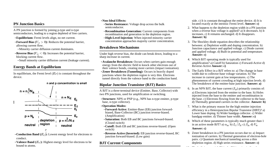
### Semiconductor Basics - **Conductors:** Materials that permit electron flow (e.g., gold, silver, copper). - **Insulators:** Materials that block electron flow (e.g., rubber, glass, Teflon). - **Semiconductors:** Materials with conductivity between conductors and insulators, whose conductivity can be controlled. - Examples: Silicon (Si), Germanium (Ge). - Conductivity (σ) is measured in mho/cm. - **Key Fact:** Silicon is the most common material for semiconductor devices. - **Silicon Properties:** - Pure silicon has 4 valence electrons. - In a crystal lattice, each Si atom forms covalent bonds with four neighbors, locking up valence electrons. - Pure Si acts as an insulator due to lack of free charge carriers. ### N-Type Silicon - **Doping:** Adding impurities to silicon to change its conductivity. - **Donor Impurities:** Pentavalent elements (5 valence electrons) like Phosphorus (P), Arsenic, Antimony, Bismuth. - **Process:** When P is added to Si, four of P's valence electrons bond with Si. The 5th electron is free to float. - **Result:** Creates N-type silicon (negative charge carrier), where free electrons migrate towards a positive voltage. - **Key Fact:** N-type silicon is doped with donor impurities. ### P-Type Silicon - **Acceptor Impurities:** Trivalent elements (3 valence electrons) like Boron (B), Aluminum, Indium, Gallium. - **Process:** When B is added to Si, its three valence electrons bond with Si, creating a "hole" (a vacant spot) in a covalent bond. - **Result:** Creates P-type silicon (positive charge carrier), where holes act as positive charge carriers, moving toward a negative voltage. - **Key Fact:** P-type silicon is doped with acceptor impurities. ### Diode Basics - **Definition:** A 2-lead semiconductor device that acts as a one-way gate for electron flow. - **Structure:** Formed by joining N-type (cathode) and P-type (anode) silicon, creating a PN-junction. - **Forward Bias:** - Anode potential > Cathode potential. - Diode conducts current. - **Water Analogy:** Water pressure from left overcomes a spring, opening a gate. - **How it Works:** Electrons from N-side and holes from P-side are forced towards the center, combine, and current flows. - **Reverse Bias:** - Anode potential - **I-V Characteristics:** - For silicon diodes, typically 0.6V or greater applied voltage is needed to conduct. ### Diode Applications #### Half-Wave Rectifier - **Function:** Converts AC input voltage to a pulsed DC output voltage. - **Operation:** Blocks current flow when AC input becomes negative at the diode's anode, making output voltage zero. - **Voltage Drop:** Introduces a 0.6V drop, so output peak is 0.6V smaller than input peak. - **Frequency:** Output frequency is the same as input frequency. #### Full-Wave Rectifier - **Function:** Transforms negative swings in input voltage into positive swings at the output. - **Bridge Circuit:** Uses four diodes (D1, D2, D3, D4). - During positive half-cycle of $V_{in}$: D3-Rout-D2 allows current flow. - During negative half-cycle of $V_{in}$: D4-Rout-D1 allows current flow. - **Voltage Drop:** Output voltage peak is 1.2V below input peak (0.6V drop for each of the two conducting diodes). - **Frequency:** Output frequency is twice the input frequency. #### AC-to-DC Power Supply - **Components:** Transformer, full-wave rectifier, filter capacitor. - **Transformer:** Steps down input voltage. - **Rectifier:** Converts AC to pulsed DC. - **Filter Capacitor:** Smooths out DC pulses. - **Condition for Steady Current:** $$R_{Load}C \gg \frac{1}{f}$$ where $f$ is the rectified signal's frequency (120Hz for 60Hz AC input). ### Transistor Basics - **Definition:** A three-lead semiconductor device that acts as an electrically controlled switch or a current amplifier. - **Analogy:** Similar to a faucet where a control knob (base current/voltage) alters water flow (larger current). #### Transistor Types - **BJT (Bipolar Junction Transistor):** - NPN and PNP types. - **NPN:** Small input current and positive voltage at base ($V_B > V_E$) allows large current from collector to emitter. - **PNP:** Small output current and negative voltage at base ($V_B - **NPN BJT Operation (OFF):** No voltage at base or negative voltage at base creates a depletion region, preventing current flow. - **NPN BJT Operation (ON):** Positive voltage ($>0.6V$) at base forward-biases the PN junction, allowing electrons to flow from emitter to collector. - **BJT Water Analogy:** - **NPN ($V_B > V_E$):** Base current opens a gate, allowing collector current to flow to emitter. - **PNP ($V_B - **NPN Transistor Circuit (OFF):** When $V_B = V_E$, no current flows from collector to emitter. - **NPN Transistor Circuit (ON):** When $V_B > V_E$, current flows from collector to emitter. - **Transistor Experiment (LED On/Off):** A simple circuit showing a transistor acting as a switch for an LED. - **JFET (Junction Field Effect Transistor):** - **Definition:** Three-lead semiconductor devices used as electrically controlled switches, current amplifiers, and voltage-controlled resistors. - **Key Feature:** Do not require a bias current; controlled by voltage. - **Operation:** Normally "on" when $V_G - V_S = 0$. When $V_G - V_S \neq 0$, JFETs become resistive to current flow. - **Types:** N-channel and P-channel. - **N-channel JFET:** Negative voltage at gate ($V_G V_S$. - **P-channel JFET:** Positive voltage at gate ($V_G > V_S$) reduces current flow from source to drain. Operates with $V_S > V_D$. - **Input Impedance:** Very high input impedance, drawing little to no input current. - **MOSFET (Metal Oxide Semiconductor FET):** - **Definition:** Similar to JFETs, but use a metal oxide insulator at the gate. - **Key Feature:** High input impedance (approx. $10^{14} \Omega$) due to insulator. Low gate-to-channel capacitance. - **Vulnerability:** Susceptible to damage from static electricity at the gate. - **Types:** Enhancement and Depletion. - **Enhancement Type:** Normally off ($V_G = V_S$). Current flow increases when $V_G \neq V_S$. - N-channel: Current increases with $V_G > V_S$. - P-channel: Current increases with $V_G V_S$. ### Optoelectronics - **Definition:** Deals with electronic devices that interact with light. - **Light Emitting Devices:** Generate electromagnetic energy (light) under electrical field (e.g., LEDs). - **Light Detecting Devices:** Transform electromagnetic energy (light) into electrical current/voltage (e.g., photoresistors, photodiodes, phototransistors). #### Light-Emitting Diodes (LEDs) - **Definition:** 2-lead PN-junction semiconductor device that emits light (visible or infrared) when forward-biased. - **Polarity:** Has specific polarity; anode must be more positive than cathode (approx. 1.4V). - **Operation:** - Forward-biased: Allows current, emits light. - Reverse-biased: Stops conducting and emitting light. - **Current Dependency:** LEDs are current-dependent devices. - Too little current: LED remains OFF. - Small current: Dimly lit. - Large current: Brightly lit. - Too much current: LED is destroyed. - **Current Control:** A resistor in series with the LED controls current. - **Formula for Series Resistor (R):** $$R = \frac{V_S - V_f}{I}$$ where $V_S$ = supply voltage, $V_f$ = forward bias voltage for LED, $I$ = desired current. - **Caution:** LEDs have limited current capacity (20mA to 100mA). - **Visible-Light LED Characteristics:** - Inexpensive, durable, used as indicator lights. - Common colors: Green (~565nm), Yellow (~585nm), Orange (~615nm), Red (~650nm). - Max forward voltage: ~1.8V. - Typical operating currents: 1 to 3mA. - Typical brightness: 1.0 to 3.0 mcd/1mA to 3.0 mcd/2mA. - **Blinking LED:** Contains an integrated circuit to flash 1-6 times/second. Used as indicator flashers or simple oscillators. - **Tricolor LED:** Two LEDs (e.g., red/orange and green) in parallel, facing opposite directions. - Current in one direction: One LED ON, other OFF. - Rapid switching: Alternates LEDs, producing yellow light. - Max voltage rating: 3V. Operating range: 10 to 20mA. - **7-Segment LED Display:** - Used for numbers/characters. 7 individual LEDs form the display. - More rugged than LCDs, but consume more power. - **How LED Works:** - PN-junction is forward-biased. Electrons from N-side combine with holes in P-side. - Photons are emitted as electrons combine with holes. - Encased in epoxy with light-scattering particles for diffusion and brightness. #### Photoresistors - **Definition:** Light-sensitive variable resistors. Resistance depends on light intensity. - **Dark Condition:** High resistance (MΩ, "dark resistance"). - **Bright Condition:** Low resistance (hundreds of Ω). - **Response Time:** - Light exposure: Resistance lowers in milliseconds. - Light removal: Resistance returns to dark state in seconds. - **Wavelength Sensitivity:** Some photoresistors respond better to specific wavelengths. - Cadmium-sulfide: 400-800nm (visible light). - Lead-sulfide: Infrared light. - **How Photoresistor Works:** - Made from semiconductor crystal (e.g., cadmium sulfide). - In dark: Electrons are strongly bound, resisting current. - In light: Photons collide with bound electrons, stripping them, creating holes. - Liberated electrons and holes contribute to current flow. - **Applications: Light-Activated Relay** - Uses a light-sensitive voltage divider to trigger a relay. - When photoresistor is exposed to light, its resistance decreases, increasing transistor base current/voltage, turning on the transistor and relay. #### Photodiode - **Definition:** 2-lead semiconductor device that transforms light energy into electric current. - **Operation:** - Wired to a current meter. - In dark: Zero current flow. - Exposed to light: Acts as a current source, causing current flow from cathode to anode. - **Characteristics:** Linear light vs. current. Often used as light meters in cameras. - **Features:** Built-in lenses/optical filters. Response time slows with increasing surface area. More sensitive than photoresistors. - **How Photodiode Works:** - A thin N-type semiconductor sandwiched with a thicker P-type semiconductor. N-side is cathode, P-side is anode. - Photons hitting the P-side collide with bound electrons, ejecting them and creating holes. - If collisions are near the PN-interface, ejected electrons cross the junction, creating extra electrons and holes. - This segregation of charges creates a potential difference. - Connecting a wire allows current to flow from anode to cathode. - **Applications: Photovoltaic Current Source** - Converts light energy directly into electric current. - Input light intensity and output current are nearly linear. #### Solar Cell - **Definition:** Photodiodes with very large surface areas. - **Advantages:** More sensitive to incoming light and yields more power (larger current/volts) than usual photodiodes. - **Output:** A single solar cell provides ~0.45-0.5V and ~0.1A in bright light. - **Basic Operation - Power Sources:** - Can be combined in series (increased voltage) or parallel (increased current) like batteries. - **Series:** Output voltage is sum of individual cell voltages. - **Parallel:** Increased output current. - **Basic Operation - Battery Charger:** - Multiple solar cells in series (e.g., nine for two 1.5V NiCd cells) can recharge batteries. - A diode prevents battery discharge through the solar cell in darkness. - A resistor can be added to slow the charge rate and prevent overcharging. #### Phototransistor - **Definition:** Light-sensitive transistor. - **Structure:** Common type replaces the base lead of a BJT with a light-sensitive surface. - **Operation:** - In darkness: Collector-emitter pair does not conduct. - Exposed to light: Small current flows from base to emitter, controlling a larger collector-emitter current. - **Alternative:** Field-effect phototransistor (Photo FET) where light exposure generates a gate voltage controlling drain-source current. - **How Phototransistor Works:** - Bipolar phototransistor has a large P-type semiconductor region exposed to light. - Photons collide with electrons in P-type region, giving them enough energy to cross the PN-junction, creating holes. - These electrons are drawn to the positive terminal, and electrons from the negative terminal combine with holes, resulting in electron current from emitter to collector. - **Applications: Light-Activated Relay** - Phototransistor controls base current of a power-switching transistor, which then controls a relay. - Light on phototransistor turns it on, allowing current to base of power-switching transistor, turning on the relay. - A 100K pot adjusts sensitivity. - **Applications: Dark-Activated Relay** - Similar circuit, but when light is *removed* from the phototransistor, it turns off, allowing *more* current to enter the base of the power-switching transistor, turning on the relay. - **Applications: Tachometer** - Uses a phototransistor as a frequency counter. - A rotating disk with a hole passes light to the phototransistor once per revolution. - Light triggers the phototransistor into conduction, generating electrical pulses. - A frequency counter counts these pulses to determine rotation speed.