Computer System Architecture (Units 4 &
Cheatsheet Content
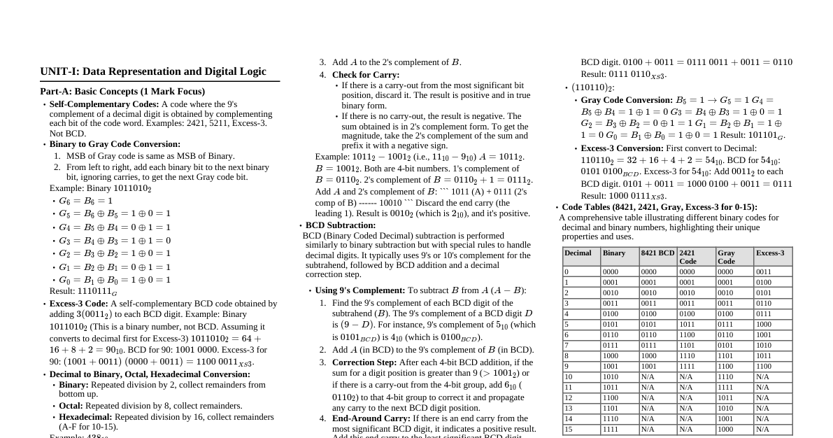
UNIT-IV: Arithmetic Operations Part-A: Short Answer Questions (1 Mark Each) 1. What is floating-point data and how to represent in a computer system? Floating-point data represents real numbers with a fractional part. It's typically represented using a sign bit ($S$), an exponent ($E$), and a mantissa ($M$), following standards like IEEE 754. The general form is $N = (-1)^S \times M \times B^E$, where $B$ is the base (usually 2). 2. Draw the flow chart for signed 2's complement addition and subtraction? A flowchart for 2's complement addition and subtraction involves converting subtraction to addition ($A - B = A + (-B)$), performing binary addition, and checking for overflow. (Visual flowchart not provided in text format, but conceptual steps are implied). 3. Draw the hardware for implementing multiplication of signed magnitude data? Hardware for signed magnitude multiplication typically includes an Accumulator, a Q register (for multiplier), a B register (for multiplicand), and control logic for shifting and adding partial products. (Visual diagram not provided). 4. Explain one stage decimal arithmetic unit? A single-stage decimal arithmetic unit performs operations on BCD (Binary Coded Decimal) digits. For addition, it adds two BCD digits and a carry-in. If the sum exceeds 9, a correction factor ($0110_2$, or 6) is added to convert it back to BCD and generate the correct carry-out. 5. Give hardware for Booth algorithm? Hardware for Booth's algorithm uses registers for the multiplicand (B), multiplier (Q), and accumulator (A), along with a 1-bit extension to Q ($Q_{-1}$). It requires an adder/subtractor unit and shift registers for arithmetic shifts based on the $Q_0 Q_{-1}$ pair. 6. Draw the block diagram for BCD adder? A BCD adder block diagram consists of a 4-bit binary adder, correction logic (to detect sum $>9$ or binary carry-out), and a second 4-bit adder to add $0110_2$ as correction when needed. (Visual diagram not provided). Part-B: Detailed Questions (10 Marks Each) 1. Explain the procedure for addition and subtraction with signed-magnitude data with the help of flowchart? Signed-Magnitude Addition/Subtraction Procedure: For signed-magnitude numbers, operations depend on the signs of the operands. Let $A$ and $B$ be two signed-magnitude numbers. Addition ($A+B$): Same Signs: Add their magnitudes ($|A| + |B|$). The sign of the result is the same as the sign of $A$. Check for overflow. Different Signs: Subtract the smaller magnitude from the larger magnitude ($||A| - |B||$). If $|A| > |B|$, the result takes the sign of $A$. If $|B| > |A|$, the result takes the sign of $B$. If $|A| = |B|$, the result is zero (usually positive sign). Subtraction ($A-B$): Subtraction is converted to addition by changing the sign of the subtrahend: $A - B = A + (-B)$. Then, perform addition as described above. For example, if $B$ is positive, $-B$ becomes negative with the same magnitude. (A flowchart would visually represent these decision points and operations.) 2. How Binary Multiplication will perform? Explain using flowchart with example? Binary Multiplication (Unsigned - Shift and Add Algorithm): Binary multiplication is performed through a series of shifts and additions of partial products. Algorithm: Initialize Product (P) = 0, Multiplier (Q), Multiplicand (M). Repeat for $n$ bits (where $n$ is the multiplier's bit length): If the LSB of Q is 1, then P = P + M. Arithmetic Right Shift P by 1 bit. Right Shift Q by 1 bit. The final product is in P (and possibly Q for the lower half of the product). Example: Multiply $1011_2 (11_{10})$ by $1101_2 (13_{10})$ M = 1011, Q = 1101, P = 0000 Step Q LSB Operation P Q Initial 0000 1101 1 1 P = P + M (0000+1011=1011) 1011 1101 Shift P, Q right 0101 0110 2 0 No addition 0101 0110 Shift P, Q right 0010 0011 3 1 P = P + M (0010+1011=1101) 1101 0011 Shift P, Q right 0110 0001 4 1 P = P + M (0110+1011=10001) 10001 0001 Shift P, Q right 1000 0000 Final Product (P concatenated with Q) = $10001111_2$ ($143_{10}$). (A flowchart would show initialization, a loop for $n$ iterations, decision for Q's LSB, add/no add, and shifts.) 3. Explain Booth multiplication algorithm for signed 2's complement data with an example? Booth's Algorithm for Signed Multiplication: Booth's algorithm efficiently multiplies signed binary numbers in 2's complement. It scans the multiplier from right to left, performing addition or subtraction based on patterns of '0's and '1's, effectively reducing the number of operations. Algorithm: Initialize Accumulator (A) = 0, Multiplier (Q), Multiplicand (M). Set $Q_{-1} = 0$. Number of iterations $n$ (bits in Q). Repeat $n$ times: Examine the pair $Q_0 Q_{-1}$ (LSB of Q and $Q_{-1}$): 00: Arithmetic Right Shift (A, Q, $Q_{-1}$) 01: A = A + M. Then Arithmetic Right Shift (A, Q, $Q_{-1}$) 10: A = A - M (A = A + (2's complement of M)). Then Arithmetic Right Shift (A, Q, $Q_{-1}$) 11: Arithmetic Right Shift (A, Q, $Q_{-1}$) The final product is in the (A, Q) registers. Example: Multiply $M = 0010_2 (+2_{10})$ by $Q = 1101_2 (-3_{10})$ using 4-bit numbers. M = 0010, -M = 1110 (2's complement of 0010) Initial: A = 0000, Q = 1101, $Q_{-1} = 0$ Count $Q_0 Q_{-1}$ Operation A Q $Q_{-1}$ Initial 0000 1101 0 1 10 A = A - M (0000 + 1110 = 1110) 1110 1101 0 ARS (A, Q, $Q_{-1}$) 1111 0110 1 2 01 A = A + M (1111 + 0010 = 0001) 0001 0110 1 ARS (A, Q, $Q_{-1}$) 0000 1011 0 3 10 A = A - M (0000 + 1110 = 1110) 1110 1011 0 ARS (A, Q, $Q_{-1}$) 1111 0101 1 4 11 ARS (A, Q, $Q_{-1}$) 1111 1010 1 The final product in (A, Q) is $11111010_2$, which is $-6_{10}$ (as expected: $2 \times -3 = -6$). 4. Explain BCD adder with its block diagram? BCD Adder: A BCD (Binary Coded Decimal) adder adds two BCD digits (4 bits each) and a carry-in to produce a BCD sum digit and a carry-out. It handles the specific rule that BCD digits must be between 0 and 9. If the sum exceeds 9, a correction is applied. Correction Logic: If the 4-bit binary sum is greater than 9 (i.e., $10_{10}$ to $18_{10}$) or if the binary adder generates a carry-out, the sum is invalid in BCD. To correct this, $0110_2$ ($6_{10}$) is added to the sum. This addition produces the correct BCD digit and generates a carry-out to the next BCD stage. Block Diagram: 4-bit Adder A (4-bit) B (4-bit) Sum (S) Cin C_binary Correction Logic Add 6? 4-bit Adder BCD Sum BCD Cout 0110 if yes, 0000 if no Operation Example: $5 + 8 = 13$ $A = 0101_2 (5)$, $B = 1000_2 (8)$, $C_{in} = 0$. First Binary Adder: $0101 + 1000 = 1101_2 (13_{10})$. $C_{binary} = 0$. Correction Logic: Sum $1101_2$ is $>9$. Correction needed. Second Binary Adder: $1101_2 + 0110_2 = (1)0011_2$. Final BCD Sum = $0011_2 (3_{10})$. BCD Carry-out = $1$. Result: BCD sum is $3$, BCD carry-out is $1$, correctly representing $13_{10}$. 5. Explain Decimal addition and subtraction with neat block diagram? Decimal Arithmetic Unit: A decimal arithmetic unit performs operations on decimal numbers, typically represented in BCD. Multi-digit operations are handled digit by digit, propagating carries. Decimal Addition: For multi-digit decimal addition, a cascade of single-digit BCD adders is used. Each BCD adder processes one pair of BCD digits and the carry-in from the previous stage, producing a sum digit and a carry-out. Block Diagram for Multi-Digit Decimal Adder: BCD Adder 0 A0 B0 S0 C1 BCD Adder 1 A1 B1 S1 C2 ... BCD Adder N AN BN SN CN+1 Cin=0 Decimal Subtraction (using 10's Complement): To compute $A - B$, we add $A$ to the 10's complement of $B$. The 10's complement of $B$ is found by taking its 9's complement and adding 1. Procedure for $A - B$: Find the 9's complement of each BCD digit of $B$. Add 1 to the least significant digit of the 9's complement to get the 10's complement of $B$. Add $A$ to the 10's complement of $B$ using a multi-digit BCD adder. If a carry-out is generated from the most significant digit, the result is positive, and the carry is discarded. If no carry-out, the result is negative. Take the 10's complement of the sum to find the magnitude and append a negative sign. Block Diagram for BCD Subtraction: 9's Compl. B0 BCD Adder 0 A0 Cin=1 S0 C1 BCD Adder 1 A1 B1 (9's Compl) S1 C2 Final Carry (Sign) 6. Explain BCD subtraction with neat block diagram? This question is a duplicate of the previous one (Decimal Subtraction). The explanation for Decimal Subtraction using 10's complement above is applicable to BCD subtraction, as BCD is the common representation for decimal arithmetic in hardware. The block diagram and procedure detailed in Part B, Question 5 for "Decimal Subtraction (using 10's Complement)" fully cover BCD subtraction. UNIT-V: Memory Organization and Pipelining Part-A: Short Answer Questions (1 Mark Each) 1. Explain Hit Ratio? The Hit Ratio is the fraction of memory accesses found in the cache. It's calculated as $\frac{Number\ of\ Hits}{Total\ Number\ of\ Accesses}$. A higher hit ratio indicates better cache performance and faster average memory access time. 2. Define mapping function and Locality of reference with respect to cache memory? Mapping Function: An algorithm that determines where a block of main memory can be placed in cache (e.g., direct, associative, set-associative). Locality of Reference: The principle that programs tend to access data and instructions that are spatially (near previously accessed data) or temporally (accessed again soon) close to recently accessed ones. Caches exploit this principle. 3. Draw and explain SRAM unit cell? An SRAM cell typically consists of 6 transistors (6T) . Two cross-coupled inverters (4 transistors) form a bistable latch to store one bit, and two access transistors control read/write operations via bit lines. (Visual diagram not provided). 4. Briefly Explain about DMA? DMA (Direct Memory Access) is a hardware feature allowing I/O devices to transfer data directly to/from main memory without CPU intervention. This frees the CPU for other tasks, significantly improving system performance for I/O-intensive operations. 5. Explain MIPS Implementation? MIPS (Microprocessor without Interlocked Pipeline Stages) refers to the hardware design executing the MIPS instruction set architecture (ISA). Key features include RISC philosophy (simple, fixed-length instructions), heavy pipelining, register-based operations, and a load/store architecture. Part-B: Detailed Questions (10 Marks Each) 1. What is the advantage of memory hierarchy? Explain main memory and memory address map. Memory Hierarchy Advantages: A memory hierarchy organizes computer memory into levels based on speed, cost, and capacity. It provides: Cost-Effectiveness: Offers large memory capacity at an affordable cost by combining small amounts of fast, expensive memory (cache) with large amounts of slower, cheaper memory (RAM, disk). Performance Improvement: Significantly reduces average memory access time by storing frequently used data in faster, higher levels (caches), leveraging locality of reference. Increased Capacity: Allows programs to utilize a virtual address space much larger than physical RAM. Simplified Management: Hardware/OS handle data movement between levels, abstracting complexity from programmers. Main Memory (RAM): Main memory, or RAM, is the primary volatile storage for programs and data actively used by the CPU. It's typically implemented with DRAM, offering uniform access time to any location. It's slower than cache but faster than secondary storage. Memory Address Map: A memory address map is a logical representation or table showing the allocation of address space to various memory and I/O devices in a computer system. It defines the specific range of physical addresses that each component (e.g., ROM, RAM modules, I/O ports) occupies. Purpose: Organizes system memory. Guides address decoding logic to prevent conflicts. Essential for hardware design and operating system development. Example: For a 16-bit address bus ($2^{16} = 65,536$ addresses), a map might be: ROM: $0000H - 0FFFH$ (4KB) RAM: $1000H - 7FFFH$ (28KB) I/O Ports: $8000H - 8FFFH$ (4KB) 2. Draw and explain the architectural features of Direct Memory Access? Direct Memory Access (DMA): DMA allows I/O devices to transfer data directly to/from main memory without CPU involvement, significantly boosting I/O performance. This is managed by a dedicated hardware component called a DMA Controller (DMAC). Architectural Features / Components of a DMAC: CPU DMA Controller Address Register Word Count Register Control Register Main Memory I/O Device Bus Request/Grant Data/Address/Control Bus DMA Control Signals DMA Controller (DMAC): Manages DMA transfers, acting as a temporary bus master. Address Register: Stores the starting memory address for transfer. Word Count Register: Stores the number of words/bytes to transfer. Control Register: Configures transfer mode (read/write, burst/cycle stealing). Bus Request (BR) / Bus Grant (BG): Signals for DMAC to request/receive bus control from CPU. Interrupt Mechanism: DMAC interrupts CPU upon transfer completion. DMA Operation (Cycle Stealing Mode): CPU programs DMAC (start address, count, direction). I/O device requests DMA to DMAC. DMAC requests bus from CPU. CPU grants bus to DMAC. DMAC takes bus control, transfers data directly between I/O device and memory, updating its registers. DMAC releases bus after each word (cycle stealing) or block (burst). DMAC interrupts CPU when transfer is complete. 3. Explain about Cache Memory and mapping process. Cache Memory: Cache is a small, fast, and expensive memory component that buffers data between the CPU and main memory. It stores frequently accessed data and instructions to reduce average memory access time, leveraging locality of reference. Modern CPUs use multi-level caches (L1, L2, L3). Cache Mapping Process: Cache mapping determines where a main memory block can be placed in the cache. It defines the translation from main memory address to cache address. 1. Direct Mapping: Each main memory block maps to exactly one specific cache line. Address is divided into: Tag | Line (Index) | Word (Offset) . Simple implementation, but prone to conflict misses if frequently used blocks map to the same line. 2. Associative Mapping (Fully Associative): Any main memory block can be placed in any cache line. Address is divided into: Tag | Word (Offset) . Highly flexible, high hit rate, but complex and expensive due to parallel tag comparison for every cache line. 3. Set-Associative Mapping: A hybrid approach. Cache is divided into sets, each containing a small number of lines. A main memory block can map to any line within a specific set. Address is divided into: Tag | Set (Index) | Word (Offset) . Offers a good balance of performance, cost, and complexity, reducing conflict misses compared to direct mapping. 4. Explain the performance considerations of a memory system? The performance of a computer system is heavily dependent on its memory system. Key considerations include: Memory Access Time (Latency): The time taken to complete a read/write operation. Lower latency means faster data retrieval. Memory Bandwidth (Throughput): The rate at which data can be transferred (bytes/second). Higher bandwidth supports data-intensive applications. Cache Hit Rate / Miss Rate: Hit Rate: Percentage of accesses found in cache. Higher is better. Miss Rate: Percentage not found in cache. Each miss incurs a penalty. Cache Miss Penalty: The extra time required to fetch data from a slower memory level (e.g., main memory) after a cache miss. Memory Capacity: The total storage amount. Sufficient main memory prevents excessive swapping to disk. Memory Technology: Different technologies (SRAM, DRAM) have varying speed, cost, power, and density characteristics. Bus Width and Speed: Determine the amount of data transferred simultaneously and the transfer rate, impacting bandwidth. Memory Controller Design: An efficient controller optimizes access patterns and scheduling. Interleaving: Dividing memory into independent banks for parallel access to increase bandwidth. Virtual Memory Performance: Page fault rate and page replacement algorithms significantly affect performance. 5. Explain Pipelining and Hazards. Pipelining: Pipelining is a CPU design technique that executes multiple instructions concurrently by breaking down instruction execution into stages (e.g., Fetch, Decode, Execute, Memory, Write-back). Like an assembly line, different stages work on different instructions simultaneously, increasing instruction throughput. Advantages: Increased instruction throughput, better hardware utilization. Hazards: Hazards are conditions that prevent an instruction from executing in its designated pipeline stage, causing stalls and reducing performance. 1. Structural Hazards: Occur when two instructions need the same hardware resource at the same time (e.g., a single memory unit for instruction fetch and data access). Resolution: Duplicate resources (e.g., separate instruction/data caches), or pipeline stalls. 2. Data Hazards: Occur when an instruction depends on the result of a prior instruction still in the pipeline. RAW (Read After Write): Most common; instruction reads a register before a previous one writes to it. Resolution: Forwarding (Bypassing): Route data directly from an earlier pipeline stage output to a later stage input. Stalling (Bubbles): Pause the pipeline until data is available. 3. Control Hazards (Branch Hazards): Occur with branch/jump instructions, where the next instruction to fetch depends on the outcome of the current instruction, which isn't known until later in the pipeline. Resolution: Stalling: Flush pipeline and refetch. Branch Prediction: Predict branch outcome and fetch speculatively. Misprediction incurs a penalty. Delayed Branch: Execute instruction immediately after branch, filling the "delay slot" with a useful, independent instruction. 6. What is virtual memory concept? Explain address mapping using pages. Virtual Memory Concept: Virtual memory is a memory management technique that gives programs the illusion of a large, contiguous, private address space, independent of the physical RAM size and fragmentation. It allows programs to use more memory than physically available by swapping inactive parts to secondary storage (disk). Benefits: Larger address space, memory protection, sharing, simplified memory management, efficient resource utilization. Address Mapping Using Pages: Virtual memory is primarily implemented through paging . Both virtual and physical memory are divided into fixed-size blocks: Pages: Blocks of the virtual address space. Page Frames: Blocks of the physical address space (RAM). Address Translation Process: The Memory Management Unit (MMU) translates a CPU-generated virtual address into a physical address . A virtual address is composed of: Virtual Page Number (VPN): Identifies the page. Page Offset: Identifies the byte/word within the page. The MMU uses a Page Table (stored in main memory, one per process) to perform this translation. CPU generates a virtual address. MMU extracts the VPN. MMU uses VPN to index into the Page Table. The entry (PTE) contains the Physical Page Frame Number (PPFN) and control bits (Valid, Dirty, Access). Page Hit: If the Valid bit is set, the page is in RAM. MMU concatenates PPFN with Page Offset to form the physical address. Page Fault: If the Valid bit is clear, the page is on disk. This triggers an OS interrupt. The OS loads the page from disk into a free page frame, updates the PTE, and restarts the instruction. A Translation Lookaside Buffer (TLB) , a small hardware cache, speeds up this process by storing recent VPN-to-PPFN mappings.