Analog and Digital Electronics
Cheatsheet Content
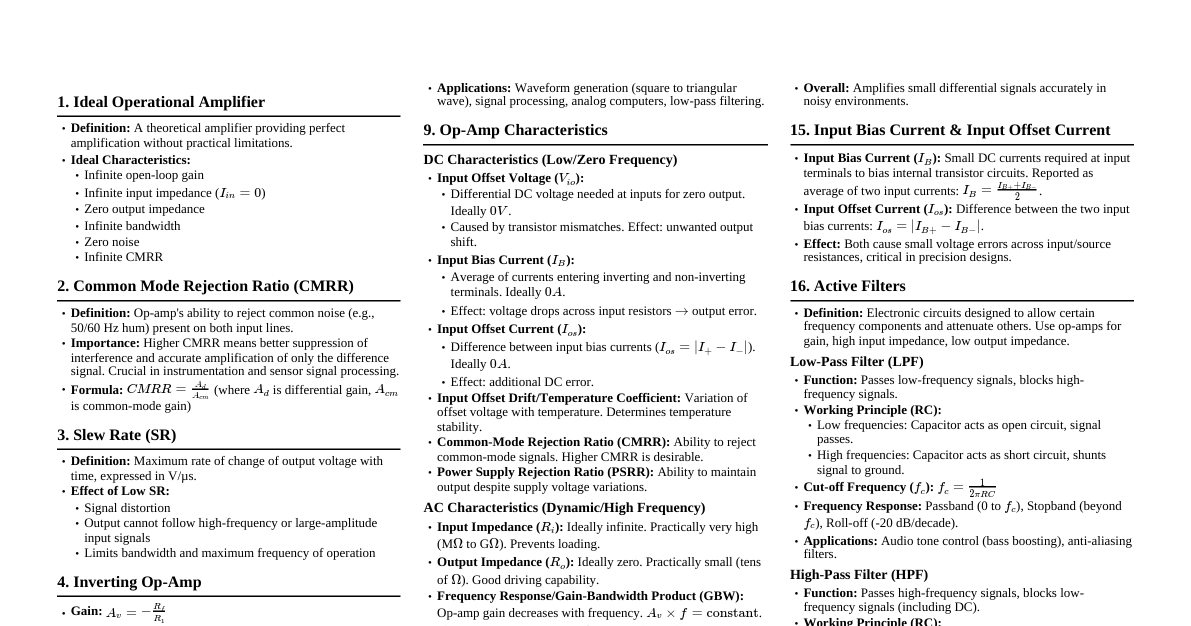
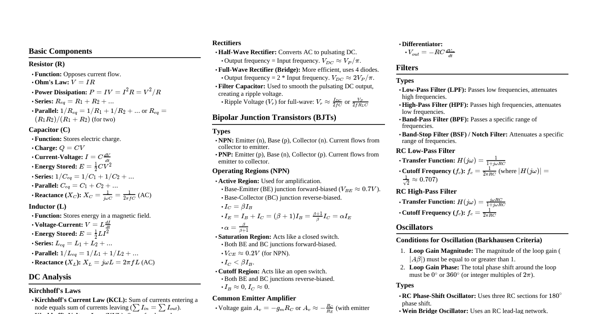
Rectifiers Rectification: Converting alternating current (AC) into direct current (DC). Rectifier Circuit: A circuit that performs rectification. Half-Wave Rectifier (HWR) Rectification occurs only for half of the AC cycle. Uses one diode. Operation: Positive half-cycle: Diode conducts, current flows, output is positive. Negative half-cycle: Diode blocks, no current flows, output is zero. HWR Disadvantages High ripple factor. Low rectification efficiency. Low transformer utilization factor. Low output power. Not typically used as a power rectifier circuit due to these limitations. HWR Applications Cheap, simple, and easy to construct. High ripple content can be used in non-critical applications like battery charging. Full-Wave Rectifier (FWR) Converts AC voltage into pulsating DC voltage using both half cycles. Center-Tapped Full-Wave Rectifier (CTFWR) Uses two diodes. Requires a center-tapped transformer. Output voltages are equal in magnitude but opposite in polarity. Operation: Positive half-cycle: One diode conducts, producing positive output. Negative half-cycle: The other diode conducts, also producing positive output. CTFWR Advantages Higher DC output power. Higher transformer utilization factor and better voltage regulation. Lower ripple content compared to HWR. CTFWR Disadvantages Center-tapping is difficult. Costly and bulky due to the complex center-tapped transformer. Requires diodes with high peak inverse voltage (PIV). Not preferred for audio applications due to ripple content. Bridge Rectifier Uses four diodes connected in a bridge form. Eliminates disadvantages of the center-tapped FWR. Operation: Positive half-cycle: Two diodes conduct. Negative half-cycle: The other two diodes conduct, current flows in the same direction through the load. Bridge Rectifier Advantages No need for center-tapping, reducing size and cost. Low ripple factor and high efficiency. DC output voltage is twice that of the center-tapped FWR. PIV of diodes is half that of the center-tapped FWR. Easier circuit design with better output. Bridge Rectifier Disadvantages Requires four diodes. Ripple Factor Definition: The ratio of the RMS value of the AC component to the DC component in the rectifier's output waveform. A measure of the quality of rectification. The AC component (ripple) is removed using a filter circuit. Voltage Regulator Definition: An electronic device or circuit that maintains a constant output voltage regardless of changes in input voltage or load conditions. Ensures sensitive electronic components receive a steady and reliable voltage. Applications: Power supplies, battery-powered devices, microcontroller circuits (Arduino, Raspberry Pi), consumer electronics, automotive systems. Operational Amplifier (Op-Amp) Circuit Symbol - + Inverting input terminal Non-inverting input terminal Output terminal Two input terminals (inverting '-' and non-inverting '+') and one output terminal. Op-Amp Characteristics (Parameters) Important for comparing performance and selecting suitable ICs. Classified into AC and DC characteristics. Key Characteristics Open-loop voltage gain: Differential gain in open-loop mode. Input resistance: Resistance measured at either input terminal with the other grounded. ($R_{in}$) Output resistance: Resistance measured at output with input source short-circuited. ($R_{out}$) Bandwidth: Range of frequencies amplified almost equally. Common-mode rejection ratio (CMRR): Ratio of differential gain to common-mode gain. Slew rate: Maximum rate of change of output voltage per unit time. Power supply rejection ratio (PSRR): Change in input offset voltage due to variation in supply voltage. Input offset voltage: Output voltage for zero input (ideally zero, practically non-zero due to unbalances). Input bias current: Average of currents flowing into input terminals. Input offset current: Algebraic difference between input currents. Ideal Op-Amp Characteristics Open-loop gain ($G$) is infinite. Input resistance ($R_{in}$) is infinite. Zero input current. Output resistance ($R_{out}$) is zero. Inverting Amplifier Output voltage is out of phase with the input voltage. Closed-loop gain ($A_{CL}$): $A_{CL} = -\frac{R_f}{R_1}$ (for ideal op-amp) Non-Inverting Amplifier Output voltage is in phase with the input voltage. Closed-loop gain ($A_{CL}$): $A_{CL} = 1 + \frac{R_f}{R_1}$ (for ideal op-amp) Voltage Follower (Buffer) A non-inverting amplifier with $R_f = 0$ and $R_1 = \infty$. Output voltage equals input voltage ($V_o = V_i$). Provides high input impedance and low output impedance. Field Effect Transistors (FETs) Definition: A unipolar device where conduction depends on majority carriers. Three terminals: Gate (G), Source (S), Drain (D). Source is analogous to BJT Emitter, Gate to BJT Base, Drain to BJT Collector. Features of FET Unipolar device. High input impedance (due to reverse bias at gate). Low output impedance. Voltage-controlled device (output voltage controlled by gate input voltage). Low noise (no junctions in conduction path). Simple to fabricate and occupies less space. Applications of FET Used in circuits to reduce loading effect. Buffer amplifiers. Phase shift oscillators. Voltmeters. Types of FETs Junction Field Effect Transistor (JFET) Metal Oxide Semiconductor Field Effect Transistor (MOSFET) MOSFET (Metal Oxide Semiconductor Field Effect Transistor) A semiconductor device for switching and amplifying electronic signals. Core of integrated circuits due to small size. Four terminals: Source (S), Gate (G), Drain (D), and Body (B). Body often connected to source, making it a three-terminal device. Gate is electrically isolated from the channel by an insulating layer (SiO$_2$), hence "Insulated Gate Field Effect Transistor". MOSFET Types Depletion-mode MOSFET (DE-MOSFET) Enhancement-mode MOSFET (E-MOSFET) N-channel Depletion MOSFET (DE-MOSFET) Consists of a lightly doped p-type substrate, with two heavily doped n-type regions (source and drain), and an n-type channel between them. A thin SiO$_2$ layer coats the surface, insulating the gate from the channel. Can operate in depletion or enhancement mode. Case 1 ($V_{GS}=0$, $V_{DS}$ fixed): Drain current ($I_D$) flows; saturation drain-source current ($I_{DSS}$) flows during pinch-off. Case 2 ($V_{GS}$ negative, $V_{DS}$ fixed - Depletion Mode): Negative gate voltage induces holes, reducing free electrons in the n-channel, thus reducing drain current. Too much negative voltage can pinch-off the channel. Case 3 ($V_{GS}$ positive, $V_{DS}$ fixed - Enhancement Mode): Positive gate voltage induces more electrons, increasing drain current. Drain Characteristics: Shows $I_D$ vs. $V_{DS}$ for different $V_{GS}$ values. Features ohmic region and constant-current source region. Transfer Characteristics: Describes $I_D$ vs. $V_{GS}$. Follows Shockley's equation: $I_D = I_{DSS} \left(1 - \frac{V_{GS}}{V_P}\right)^2$. Applications: Constant current source, voltage variable resistor. N-channel Enhancement MOSFET (E-MOSFET) Consists of a lightly doped p-type substrate, with two heavily doped n-type regions (source and drain), but no diffused channel between them initially. A thin SiO$_2$ layer coats the surface. Operates only in enhancement mode (normally-off). Does not conduct when $V_{GS}=0$. Operation: When drain is positive and gate is zero, small reverse leakage current flows. When gate is positive, negative charge carriers (electrons) are induced in the substrate, forming an n-type channel. As $V_{GS}$ increases, more electrons accumulate, and drain current flows. Drain Characteristics: Shows $I_D$ vs. $V_{DS}$ for different $V_{GS}$ values. Lowest curve is at $V_{GS(TH)}$ (threshold voltage). Transfer Characteristics: Shows $I_D$ vs. $V_{GS}$. Current increases slowly at first, then rapidly with $V_{GS}$. Applications: Switch, amplifiers, choppers, linear voltage regulators. Bipolar Junction Transistors (BJTs) Definition: A three-terminal device (Base, Emitter, Collector) where operation depends on both majority and minority carriers ("bipolar"). Can be used for voltage and current amplification. Has two p-n junctions: Emitter-Base Junction (EBJ) and Collector-Base Junction (CBJ). Input signal applied to the base is amplified at the collector. Transistor Construction Emitter: Heavily doped region that supplies charge carriers. Collector: Moderately doped region that collects charge carriers. Base: Lightly doped, thin middle region that controls charge carrier flow. Types of BJTs NPN Transistor: Emitter (n), Base (p), Collector (n). Electrons are majority carriers. PNP Transistor: Emitter (p), Base (n), Collector (p). Holes are majority carriers. Doping Levels Emitter doping is highest ($\sim 10^{15}$). Collector doping is intermediate ($\sim 10^7 - 10^8$). Base doping is lowest ($\sim 10^6$). Biasing of Transistor For proper operation: Emitter-Base Junction (EBJ) is forward biased. Collector-Base Junction (CBJ) is reverse biased. Forward bias at EBJ reduces depletion region; reverse bias at CBJ increases it. Emitter current ($I_E$) = Base current ($I_B$) + Collector current ($I_C$). Modes of Transistor Operation Mode EB Junction CB Junction Active Forward Reverse Cut-off Reverse Reverse Saturation Forward Forward Active Region: Used as an amplifier. Cut-off Mode: Acts as an open switch (nearly zero current). Saturation Mode: Acts as a closed switch (large collector current). Transistor Circuit Configurations Common Base (CB) / Grounded Base: Base is common to input and output. Common Emitter (CE) / Grounded Emitter: Emitter is common to input and output. Common Collector (CC) / Grounded Collector: Collector is common to input and output. Common Emitter (CE) Configuration Emitter is common to both input and output signals. Input applied between base and emitter; output taken between collector and emitter. Produces highest current and power gain among BJT configurations. Input impedance is low (forward-biased PN-junction). Output impedance is high (reverse-biased PN-junction). Used when large current gain is needed. CE Input Characteristics ($I_B$ vs. $V_{BE}$) Shows relationship between base current ($I_B$) and base-emitter voltage ($V_{BE}$). $I_B$ is on y-axis, $V_{BE}$ on x-axis. Output voltage ($V_{CE}$) is kept constant. Behaves like a normal p-n diode characteristic. After $\approx 0.7V$, $I_B$ increases rapidly with $V_{BE}$. In CE, $I_B$ is small (microamperes) because the base is lightly doped and thin. CE Output Characteristics ($I_C$ vs. $V_{CE}$) Shows relationship between collector current ($I_C$) and collector-emitter voltage ($V_{CE}$). $I_C$ is on y-axis, $V_{CE}$ on x-axis. Input current ($I_B$) is kept constant. Regions: Cut-off Region: $I_B = 0 \mu A$. Both junctions reverse biased. Active Region: Emitter-base forward biased, collector-base reverse biased. Used for amplification. Saturation Region: Both junctions forward biased. $V_{CE}$ is small ($\approx 0.2V$), $I_C$ increases rapidly. Transistor Parameters (CE Configuration) Forward Current Gain ($\beta$): $\beta = \frac{\Delta I_C}{\Delta I_B}$ High in CE configuration, used for current amplification. Reverse Voltage Gain ($h_{re}$): $h_{re} = \frac{\Delta V_{BE}}{\Delta V_{CE}}$ (at constant $I_B$) Dynamic Input Resistance ($r_i$): $r_i = \frac{\Delta V_{BE}}{\Delta I_B}$ (at constant $V_{CE}$) Low in CE configuration. Dynamic Output Resistance ($r_o$): $r_o = \frac{\Delta V_{CE}}{\Delta I_C}$ (at constant $I_B$) High in CE configuration. Relation between $\beta$ and $\alpha$ $\alpha = \frac{\Delta I_C}{\Delta I_E}$ (common base current gain) $\beta = \frac{\alpha}{1-\alpha}$ $I_E = I_B + I_C$ Collector Current ($I_C$) Equation $I_C = \beta I_B + I_{CEO}$ (where $I_{CEO}$ is collector-emitter leakage current with base open) Applications of BJT (CE Configuration) Amplifiers (provides voltage and current gain). Oscillator circuits. Switches in digital circuits. Electronic equipment: mobile phones, industrial control, television, radio transmitters, computers, satellites.