Analog and Digital Integrated Circuits
Cheatsheet Content
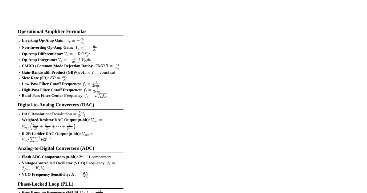
1. Ideal Operational Amplifier Definition: A theoretical amplifier providing perfect amplification without practical limitations. Ideal Characteristics: Infinite open-loop gain Infinite input impedance ($I_{in} = 0$) Zero output impedance Infinite bandwidth Zero noise Infinite CMRR 2. Common Mode Rejection Ratio (CMRR) Definition: Op-amp's ability to reject common noise (e.g., 50/60 Hz hum) present on both input lines. Importance: Higher CMRR means better suppression of interference and accurate amplification of only the difference signal. Crucial in instrumentation and sensor signal processing. Formula: $CMRR = \frac{A_d}{A_{cm}}$ (where $A_d$ is differential gain, $A_{cm}$ is common-mode gain) 3. Slew Rate (SR) Definition: Maximum rate of change of output voltage with time, expressed in V/µs. Effect of Low SR: Signal distortion Output cannot follow high-frequency or large-amplitude input signals Limits bandwidth and maximum frequency of operation 4. Inverting Op-Amp Gain: $A_v = -\frac{R_f}{R_1}$ Input Impedance: Low ($R_1$) Phase Shift: $180^\circ$ inversion Input Reference: Virtual ground (inverting input held at $0V$) Example Calculation: Given: $R_1 = 10k\Omega$, $R_f = 47k\Omega$, $V_{in(pp)} = 2V$ $A_v = -\frac{47k}{10k} = -4.7$ $V_{o(pp)} = |-4.7| \times 2V = 9.4V$ $V_{o(rms)} = \frac{V_{pp}}{2\sqrt{2}} = \frac{9.4}{2.828} \approx 3.32V$ 5. Non-Inverting Op-Amp Gain: $A_v = 1 + \frac{R_f}{R_1}$ Input Impedance: Very high (approaching ideal op-amp's infinite input impedance) Phase Shift: No inversion Input Reference: Direct input to non-inverting terminal 6. Voltage Follower (Buffer) Configuration: Non-inverting op-amp with $R_f = 0$ (short circuit) and $R_1 = \infty$ (open circuit). Output directly connected to inverting input. Gain: $A_v = 1$ Input Impedance: Extremely high due to 100% negative feedback and no resistor at input terminal, resulting in almost zero input current. Ideal for buffering. Output Impedance: Very low. 7. Differentiator Op-Amp Circuit Definition: Produces an output voltage proportional to the rate of change (derivative) of the input signal. Output Voltage: $V_o = -RC \frac{dV_{in}}{dt}$ Circuit Diagram: C $R_f$ $V_{in}$ $V_o$ - + Applications: Edge detection, FM demodulation, pulse shaping, high-pass filtering. 8. Integrator Op-Amp Circuit Definition: Produces an output voltage proportional to the time integral of the input signal. Output Voltage: $V_o = -\frac{1}{RC} \int V_{in} dt$ Circuit Diagram: $R_1$ $C_f$ $V_{in}$ $V_o$ - + Applications: Waveform generation (square to triangular wave), signal processing, analog computers, low-pass filtering. 9. Op-Amp Characteristics DC Characteristics (Low/Zero Frequency) Input Offset Voltage ($V_{io}$): Differential DC voltage needed at inputs for zero output. Ideally $0V$. Caused by transistor mismatches. Effect: unwanted output shift. Input Bias Current ($I_B$): Average of currents entering inverting and non-inverting terminals. Ideally $0A$. Effect: voltage drops across input resistors $\to$ output error. Input Offset Current ($I_{os}$): Difference between input bias currents ($I_{os} = |I_+ - I_-|$). Ideally $0A$. Effect: additional DC error. Input Offset Drift/Temperature Coefficient: Variation of offset voltage with temperature. Determines temperature stability. Common-Mode Rejection Ratio (CMRR): Ability to reject common-mode signals. Higher CMRR is desirable. Power Supply Rejection Ratio (PSRR): Ability to maintain output despite supply voltage variations. AC Characteristics (Dynamic/High Frequency) Input Impedance ($R_i$): Ideally infinite. Practically very high (M$\Omega$ to G$\Omega$). Prevents loading. Output Impedance ($R_o$): Ideally zero. Practically small (tens of $\Omega$). Good driving capability. Frequency Response/Gain-Bandwidth Product (GBW): Op-amp gain decreases with frequency. $A_v \times f = \text{constant}$. Slew Rate (SR): Max rate of output voltage change ($SR = \frac{dV_o}{dt}$). Limits speed of response. Rise Time & Settling Time: Time for output to reach/settle to final value. Crucial for high-speed systems. Phase Margin & Stability: Indicates system stability (ringing/oscillation). Unity Gain Frequency ($f_u$): Frequency where open-loop gain is 1. Higher $f_u$ means faster op-amp. Input Capacitance: Internal capacitances affecting high-frequency behavior. Output Voltage Swing: Max positive/negative output without distortion. Limited by supply rails. Total Harmonic Distortion (THD): Distortion when amplifying AC signals. Lower THD $\to$ higher fidelity. 10. Open-Loop Op-Amp Configurations (Comparators) Unsuitable for Linear Applications: Extremely high open-loop gain ($>10^5$) causes even small input differences to drive output to saturation (digital-like output). Use: Primarily as comparators (digital applications), not linear amplifiers. 11. Virtual Ground Definition: In an inverting op-amp with negative feedback, the inverting input is held at $0V$ (ground potential) without being physically grounded. Importance: Ensures linear operation and accurate gain calculations. 12. Voltage-to-Current (V-I) Converter Applications Driving LEDs and laser diodes Industrial 4-20 mA current loop transmitters Measuring transducer outputs Biomedical sensors and actuators 13. 741 Op-Amp Limitations for High Frequencies Low Gain-Bandwidth Product (GBW): Typical $\approx 1MHz$, limiting closed-loop bandwidth. Low Slew Rate: $\approx 0.5V/\mu s$, cannot reproduce fast edges without distortion. Poor Input Stages: Requires dual $\pm$ supply. No Internal Frequency Compensation: Outdated internal transistor technology. Result: Distorts and attenuates signals at high frequencies. Modern op-amps (high-speed designs) are preferred. 14. Instrumentation Amplifier Purpose: High-precision differential amplifier for amplifying very small differential signals in noisy environments. Advantages: Very high input impedance (doesn't load sensors). High Common-Mode Rejection Ratio (CMRR) to suppress interference and supply/ground shifts. Accurate, stable gain (adjustable by a single resistor for calibration). Low offset and drift versions available for small differential signals (e.g., biomedical ECG, thermocouples, strain gauges). Overall: Amplifies small differential signals accurately in noisy environments. 15. Input Bias Current & Input Offset Current Input Bias Current ($I_B$): Small DC currents required at input terminals to bias internal transistor circuits. Reported as average of two input currents: $I_B = \frac{I_{B+} + I_{B-}}{2}$. Input Offset Current ($I_{os}$): Difference between the two input bias currents: $I_{os} = |I_{B+} - I_{B-}|$. Effect: Both cause small voltage errors across input/source resistances, critical in precision designs. 16. Active Filters Definition: Electronic circuits designed to allow certain frequency components and attenuate others. Use op-amps for gain, high input impedance, low output impedance. Low-Pass Filter (LPF) Function: Passes low-frequency signals, blocks high-frequency signals. Working Principle (RC): Low frequencies: Capacitor acts as open circuit, signal passes. High frequencies: Capacitor acts as short circuit, shunts signal to ground. Cut-off Frequency ($f_c$): $f_c = \frac{1}{2\pi RC}$ Frequency Response: Passband (0 to $f_c$), Stopband (beyond $f_c$), Roll-off (-20 dB/decade). Applications: Audio tone control (bass boosting), anti-aliasing filters. High-Pass Filter (HPF) Function: Passes high-frequency signals, blocks low-frequency signals (including DC). Working Principle (RC): Low frequencies: Capacitor acts as open circuit, blocks signal. High frequencies: Capacitor acts as short circuit, signal passes. Cut-off Frequency ($f_c$): $f_c = \frac{1}{2\pi RC}$ Frequency Response: Blocked region (0 to $f_c$), Passband (above $f_c$), Roll-off (+20 dB/decade). Applications: Removing DC drift (EEG, ECG), coupling AC signals, audio treble enhancement, edge detection. Band-Pass Filter (BPF) Function: Allows a specific range of frequencies to pass, attenuates others. Types: Wide Bandpass Filters: Combine characteristics of HPF and LPF. Often created by cascading an LPF and an HPF. Narrow Bandpass Filters: Allow a tiny frequency range, often use multiple feedback loops. Center Frequency ($F_c$): Geometric mean of low and high cutoff frequencies ($F_c = \sqrt{F_L F_H}$). Bandwidth (BW): $BW = F_H - F_L$. Applications: Radio receivers, biomedical monitors. Band-Stop Filter (Notch Filter) Function: Removes a specific range of frequencies (e.g., 50 Hz hum). 17. Schmitt Trigger Definition: A regenerative comparator circuit with positive feedback, exhibiting hysteresis. Hysteresis: Property where switching thresholds for rising ($V_{TH+}$) and falling ($V_{TH-}$) inputs are different. Prevents chatter and false triggering due to noise or slow input transitions. Hysteresis Width: $V_{Hyst} = V_{TH+} - V_{TH-}$ Upper Threshold: $V_{TH+} = +V_{sat} \frac{R_2}{R_1+R_2}$ Lower Threshold: $V_{TH-} = -V_{sat} \frac{R_2}{R_1+R_2}$ Function: Converts noisy/slow analog signals into sharp digital outputs (squaring circuit). 18. Multivibrators Definition: Electronic circuits used to implement two-state systems like oscillators, timers, and flip-flops. Astable Multivibrator Stable States: None (continuously oscillates). Output: Continuous square/pulse train. Trigger: Self-triggered (no external input). Uses: Clock/pulse generation, tone generation. Example: 555 astable for clock. Monostable Multivibrator (One-Shot) Stable States: One stable state, one quasi-stable state. Output: Single pulse per trigger. Trigger: Requires external trigger to start pulse. Uses: Timers, missing-pulse detection, one-shot timing. Example: 555 monostable for one-shot delay. Working Principle: Assumes output $V_o = +V_{sat}$ (stable state). Diode $D_1$ clamps capacitor voltage to $0.7V$. Negative trigger $V_T$ applied to non-inverting input $\to$ effective voltage less than $0.7V$. Output switches to $-V_{sat}$ (quasi-stable state). Diode $D_1$ reverse biased, capacitor charges exponentially towards $-V_{sat}$. When capacitor voltage reaches $- \beta V_{sat}$, output switches back to $+V_{sat}$. Capacitor discharges, returns to $0.7V$. 19. Weighted-Resistor DAC Definition: Converts digital word into analog output using resistors weighted according to powers of two ($R, 2R, 4R, \dots$). Working Principle: Each digital bit controls a switch, current contribution from each resistor is summed, output voltage proportional to digital input. Resolution: Smallest change in analog output for a one-bit change in input. $Resolution = \frac{V_{ref}}{2^n-1}$. Advantage: Simple concept. Limitation: Requires wide range of precise resistor values, difficult to fabricate accurately for high resolution. 20. R-2R Ladder DAC Definition: Converts digital word into analog output using only two resistor values ($R$ and $2R$) in a ladder network. Advantage: Requires only two resistor values, easier to fabricate accurately (better matching $\to$ improved linearity), easier IC implementation. Limitation: Slightly slower due to ladder network and switching delays. 21. Flash ADC Operating Principle: Uses a resistor ladder to generate reference voltages and compares input simultaneously with all reference levels using comparators. Speed: Fastest ADC architecture because entire conversion happens in one step, no clock cycles needed for conversion. Comparators: For $n$-bit ADC, $2^n-1$ comparators are needed. Conversion Delay: Time required for comparators to respond. 22. Successive Approximation Register (SAR) ADC Definition: Converts analog input by comparing it with outputs from an internal DAC using a binary search algorithm. Key Advantage: Excellent balance between speed and accuracy. Faster than integrating ADCs, more accurate than flash ADCs. Building Blocks: Sample and Hold circuit, Comparator, SAR, Digital-to-Analog Converter (DAC). 23. Dual-Slope ADC Advantages (precision measurement): High accuracy and excellent noise rejection. Insensitive to component variations (R, C stability). 24. Voltage-Controlled Oscillator (VCO) Definition: Oscillator whose output frequency varies linearly with an applied control voltage. Output Frequency: $f_o = f_{free} + K_v V_c$ (where $f_{free}$ is free-running frequency, $K_v$ is frequency sensitivity, $V_c$ is control voltage). Frequency Sensitivity ($K_v$): Change in output frequency per unit change in control voltage. Units: Hz/V or rad/s/V. Types: Harmonic (sinusoidal waveform, e.g., crystal oscillators), Relaxation (sawtooth/triangular waveform, wide frequency range). Applications: Function generators, FM modulation, frequency shift keying, clock generators. 25. Phase-Locked Loop (PLL) Definition: Closed-loop control system that locks the phase and frequency of a VCO to an input reference signal. Working Principles: Phase Detector: Compares input frequency ($f_i$) with feedback frequency ($f_o$). Produces an error voltage proportional to phase difference. Loop Filter (LPF): Filters out high-frequency components from phase detector output, producing a steady DC control voltage. Voltage-Controlled Oscillator (VCO): Generates an output frequency controlled by the loop filter's DC voltage. Feedback Loop: VCO output is fed back to the phase detector, closing the loop. Lock Range ($f_L$): Range of frequencies over which the PLL can maintain lock. For NE/SE 565: $f_L = \pm \frac{8f_o}{V_{CC}}$. Capture Range ($f_C$): Range of frequencies over which the PLL can acquire lock. $f_C \approx \frac{f_L}{\sqrt{2}}$. Applications: FM demodulation. Frequency synthesizers (for generating multiple output frequencies). Clock recovery/data synchronization. Motor speed control. Frequency multiplication. 26. Number Systems & Codes 1's and 2's Complement 1's Complement: Invert all bits (0 to 1, 1 to 0). 2's Complement: 1's complement + 1. Example: For binary $011010_2$: 1's complement: $100101_2$ 2's complement: $100101_2 + 1 = 100110_2$ Gray Code Definition: A binary numeral system where two successive values differ in only one bit. Conversion (Binary to Gray): MSB is the same. Subsequent bits are XORed with the previous binary bit. Example: For binary $10110_2$: MSB: 1 $1 \oplus 0 = 1$ $0 \oplus 1 = 1$ $1 \oplus 1 = 0$ $1 \oplus 0 = 1$ Gray code: $11101_G$ BCD (Binary Coded Decimal) 8421 BCD: Each decimal digit is represented by its 4-bit binary equivalent. Example: Decimal 9 in 8421 BCD is $1001_2$. Excess-3 Code Conversion: Add 3 ($0011_2$) to each decimal digit's 4-bit BCD representation. Example: For decimal 59: 5: $0101_2 + 0011_2 = 1000_2$ 9: $1001_2 + 0011_2 = 1100_2$ Excess-3 for 59: $1000 \ 1100_{XS3}$ Alphanumeric Code Definition: Sequence using letters (A-Z, a-z), numbers (0-9), and often symbols (!@#$). Use: Identification, passwords, product codes. 27. Boolean Algebra & Logic Gates De Morgan's Theorems First Theorem: Complement of a product is the sum of the complements. $(A \cdot B)' = A' + B'$. Second Theorem: Complement of a sum is the product of the complements. $(A + B)' = A' \cdot B'$. SOP (Sum of Products) Form Definition: Sum (OR) of product (AND) terms (minterms). Focuses on '1' outputs. Minterm: A product term including all variables (true or complemented) that is '1' for exactly one input combination. Example: $F = A'B' + AB' + AB$ (for $\Sigma m(0,2,3)$ with A,B variables) POS (Product of Sums) Form Definition: Product (AND) of sum (OR) terms (maxterms). Focuses on '0' outputs. Maxterm: A sum term including all variables (true or complemented) that is '0' for exactly one input combination. Example: $F = (A+B')(A'+B)(A'+B')$ (for $\Pi M(1,4,6)$ with A,B,C variables) Universal Gates (NAND, NOR) Definition: NAND and NOR gates are universal because any Boolean function (AND, OR, NOT, XOR) can be implemented using only one type of these gates. Boolean Simplification Prime Implicant: A product term that cannot be combined further to eliminate variables. Essential Prime Implicant: A prime implicant that covers at least one minterm not covered by any other prime implicant. Karnaugh Maps (K-Maps) Purpose: Graphical method to simplify Boolean expressions. Process: Map minterms/maxterms and don't care conditions, group adjacent 1s (for SOP) or 0s (for POS) in powers of 2. 28. Combinational Logic Circuits Definition: Digital circuits whose outputs depend only on the current inputs. Design Steps: Define Inputs and Outputs. Create Truth Table. Derive Boolean Expressions (SOP/POS). Simplify Boolean Expressions (K-Maps/Algebra). Implement Logic Diagram. Types: Adders, Subtractors, Multiplexers, Demultiplexers, Encoders, Decoders, Comparators. Half Adder Function: Adds two 1-bit binary digits. Outputs: Sum ($S = A \oplus B$) Carry ($C_{out} = A \cdot B$) Full Adder Function: Adds three 1-bit binary digits (A, B, $C_{in}$). Outputs: Sum ($S = A \oplus B \oplus C_{in}$) Carry ($C_{out} = (A \cdot B) + (C_{in} \cdot (A \oplus B))$) Implementation: Can be constructed using two half adders and one OR gate. Carry Look-Ahead Adders: Reduce carry propagation delay by calculating carry signals in advance. Half Subtractor Function: Subtracts two 1-bit binary digits. Outputs: Difference ($D = A \oplus B$) Borrow ($B_{out} = A' \cdot B$) Full Subtractor Function: Subtracts three 1-bit binary digits (Minuend A, Subtrahend B, Borrow-in $B_{in}$). Outputs: Difference ($D = (A \oplus B) \oplus B_{in}$) Borrow-out ($B_{out} = A'B + A'B_{in} + BB_{in}$) BCD Adder Function: Adds BCD numbers. Handles decimal digits (0-9). Design Steps: Find number of digits, full-adder structure, BCD correction (add 0110 if sum > 9 or carry generated). Advantages: Decimal precision, simplified decimal arithmetic, display compatibility. Multiplexer (MUX) Function: Selects one of several input data lines and routes it to a single output based on select lines. Also called a data selector. Applications: Data routing, communication systems (combining signals), memory interfacing, logic function implementation. Demultiplexer (DEMUX) Function: Receives data on a single line and transmits it to one of $2^n$ possible output lines based on $n$ select lines. Applications: Data routing in communication systems (separating combined signals), memory address decoding. Decoder as DEMUX: A decoder can function as a demultiplexer if its enable input is used as the data input and select lines determine the output. Digital Comparator Function: Compares two binary numbers (A, B) and indicates their relationship ($A=B, A>B, A 1-bit Equality Comparator: Uses an XNOR gate ($A \odot B = A'B' + AB$). Output is HIGH (1) if inputs are equal. Encoder Function: Converts multiple input signals into a binary code. Priority Encoder: Encodes multiple inputs into a binary output, giving importance to the highest-priority active input. Applications: Keyboard encoding, data compression. Decoder Function: Converts an $n$-bit binary input into a unique output line (out of $2^n$ possible lines). Applications: Memory address decoding, display systems (e.g., 7-segment displays). 29. Sequential Logic Circuits Definition: Digital circuits whose outputs depend on both current inputs and previous states. Classification: Clocking (Timing): Synchronous (state changes only on clock pulses), Asynchronous (state changes immediately with input changes). Output Dependence: Moore Machine (output depends only on present state), Mealy Machine (output depends on present state and input). Memory Elements: Latch-based (level-sensitive), Flip-flop-based (edge-triggered). Latches vs. Flip-Flops Latch: Level-sensitive: Output changes as long as enable signal is active. No clock signal required, responds immediately to input changes. Simpler, faster, but more prone to timing problems. Used in asynchronous circuits. Flip-Flop: Edge-triggered: Output changes only on rising or falling edge of clock. Requires a clock signal to control state changes. More reliable, stable in synchronous systems. Used in synchronous circuits (counters, registers). SR Flip-Flop Inputs: Set (S), Reset (R), Clock. Outputs: Q, Q' (complement of Q). Operation: S=0, R=0: Hold (Q unchanged). S=0, R=1: Reset (Q=0). S=1, R=0: Set (Q=1). S=1, R=1: Invalid state (both Q and Q' attempt to be 1). Characteristic Equation: $Q_{n+1} = S + R'Q_n$ (for valid states). Implementation: Can be built using NAND or NOR gates. JK Flip-Flop Inputs: J, K, Clock. Outputs: Q, Q'. Operation: J=0, K=0: Hold (Q unchanged). J=0, K=1: Reset (Q=0). J=1, K=0: Set (Q=1). J=1, K=1: Toggle (Q changes state). This resolves the invalid state of SR flip-flop. Characteristic Equation: $Q_{n+1} = JQ_n' + K'Q_n$. Excitation Table: Shows J, K inputs required for a desired state transition (Qn to Qn+1). Race-Around Condition: Occurs if J=K=1 and clock pulse is too long, causing output to toggle multiple times. Can be avoided with edge-triggering or Master-Slave JK flip-flop. Frequency Division: For J=K=1, the output frequency is half the clock frequency. D Flip-Flop Inputs: Data (D), Clock. Outputs: Q, Q'. Operation: The output Q follows the input D on the active clock edge. $Q_{n+1} = D$. Purpose: Used for data storage/delay. Conversion to T-Flip-Flop: Connect $D = T \oplus Q$. T Flip-Flop Inputs: Toggle (T), Clock. Outputs: Q, Q'. Operation: T=0: Hold (Q unchanged). T=1: Toggle (Q changes state). Characteristic Equation: $Q_{n+1} = T \oplus Q_n = TQ_n' + T'Q_n$. Applications: Counters, frequency dividers. State Assignment Definition: Assigning binary codes to the states of a sequential circuit. Significance: Minimizes hardware complexity, improves circuit speed, simplifies design, ensures correct operation. Shift Registers Definition: A cascade of flip-flops used to store and shift binary data. Types: Serial-in, Serial-out (SISO) Serial-in, Parallel-out (SIPO) Parallel-in, Serial-out (PISO) Parallel-in, Parallel-out (PIPO) Universal Shift Register: Can perform all shift operations (shift left, shift right, parallel load, hold). Applications: Serial-to-parallel/parallel-to-serial conversion, data storage/delay, counters, sequence generators. Counters Definition: Sequential circuits that count a specific sequence of states. Mod-N Counter: Counts N distinct states. Requires $n$ flip-flops where $2^n \ge N$. Synchronous Counter: All flip-flops are clocked simultaneously with a common clock. Asynchronous Counter (Ripple Counter): Output of one flip-flop acts as clock for the next. Ring Counter: A shift register where the output of the last flip-flop is fed back to the input of the first. Produces $N$ unique states for $N$ flip-flops. Johnson Counter (Twisted Ring Counter): A ring counter where the inverted output of the last flip-flop is fed back to the input of the first. Produces $2N$ unique states for $N$ flip-flops. Mealy vs. Moore Machines Mealy Machine: Output depends on both present state and present input. Faster response, fewer states. Moore Machine: Output depends only on present state. More stable output, more states.