Digital Logic & Design (19-30)
Cheatsheet Content
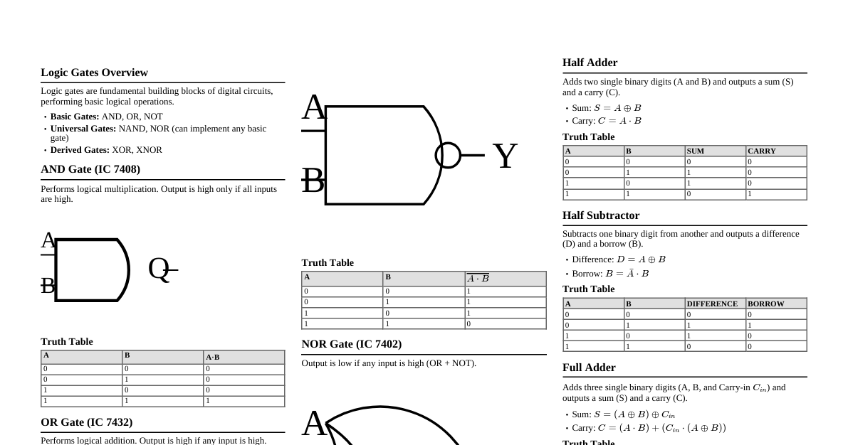
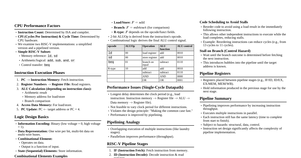
### Demultiplexers (Lesson 19) - **Function:** Routes a single input to one of several outputs. Also known as Data Distributors. - **Circuit:** Similar to a decoder, where the decoder's enable input acts as the demultiplexer's data input. - **Applications:** - Connecting a single source (e.g., ALU output) to multiple destinations (e.g., registers). - **Serial-to-Parallel Conversion:** Incoming serial data stream is routed to successive outputs (storage elements) to reconstruct parallel data. ### Programmable Logic Devices (PLDs) (Lesson 19) - **Purpose:** Replace logic gates and MSI chips, saving space and cost. - **Structure:** Consist of arrays of AND gates and OR gates that can be programmed. - **Arrays:** - **Grid:** Conductors forming rows and columns, with fuses connecting intersections. - **Programming:** Fuses are blown (or shorted) to disconnect (or connect) specific paths. - **Input Buffers:** Provide both true and complemented forms of input variables. - **Simplified Diagram:** Single line with a slash indicates multiple AND gate inputs; 'X' marks intact fuses (connections). #### Types of PLDs 1. **Programmable Read-Only Memory (PROM)** - **Architecture:** Fixed (non-programmable) AND array (decoder) + Programmable OR array. - **Use:** Primarily as a storage device, not a logic device. 2. **Programmable Logic Array (PLA)** - **Architecture:** Programmable AND array + Programmable OR array. - **Flexibility:** Overcomes PROM limitations, user-programmable (Field-Programmable Logic Array). - **Limitations:** Defined by number of inputs (n), outputs (m), and product terms (p) (n x m PLA with p product terms). - **Programming for 0/1 Output:** - Constant 0: Connect a variable AND its complement to an AND gate (e.g., `A & !A`). - Constant 1: Leave all inputs to an AND gate disconnected (produces logical 1). 3. **Programmable Array Logic (PAL)** - **Architecture:** Programmable AND array + Fixed OR array. - **Advantage:** Simpler than PLA, overcoming PLA's longer delays and complex circuitry. - **Output Logic:** Can be configured as: - **Combinational Output:** Active-high or active-low. - **Combinational Input/Output:** Output can feed back to input array or act as an input pin. - **Programmable Polarity Output:** Uses an XOR gate at the output to select function or its complement. - **Identification:** `PAL L/H/P ` (e.g., PAL10L8). 4. **Generic Array Logic (GAL)** - **Architecture:** Reprogrammable AND array + Fixed OR array + Programmable Output Logic (OLMC). - **Technology:** Uses E2CMOS (Electrically Erasable CMOS) instead of fuses, allowing reprogramming. - **OLMCs:** Output Logic Macro Cells can be programmed for combinational or registered logic. - **GAL22V10:** Popular GAL with 12 inputs, 10 I/O pins, and 10 OLMCs (varying product term inputs: 8, 10, 12, 14, 16). - **GAL16V8:** 8 inputs, 2 special function inputs, 8 I/O pins. Emulates most PALs (Simple, Complex, Registered modes). ### PLD Programming (Lesson 20) - **Process:** Computer with programming software connects to a PLD programmer. - **Input:** Logic function as Boolean equation, truth table, or state diagram. - **Software:** Compiles input file, minimizes logic, tests with test vectors. - **Output:** Documentation file, JEDEC file (downloaded to programmer). - **In-System Programming (ISP):** Program PLDs after installation on a circuit board via a 4-wire interface. ### ABEL (Advanced Boolean Expression Language) (Lesson 20-21) - **Purpose:** Device-independent hardware description language for PLDs. - **Methods for Logic Design:** - Boolean Equations - Truth Tables - State Diagrams (for Sequential Logic) - **Syntax:** - **Operators:** `!` (NOT), `&` (AND), `#` (OR), `$` (XOR). Precedence: `!`, `&`, `#`, `$`. - **Equations:** End with `;`. Case-sensitive. - **Sets:** Group multiple bits (e.g., `D = [D0, D1, D2];`). - **Relational Operator:** `==` (e.g., `(S == 0)`). - **ABEL Input File Structure:** 1. **Declarations:** Device (`device 'P20V8';`), pin (`A0, A1, A2, A3 pin 1, 2, 3, 4;`), set (`INPUT = [A1, A0, B1, B0];`). 2. **Logic Descriptions:** Boolean equations or truth tables. 3. **Test Vectors:** Specify inputs and expected outputs for verification. ### Sequential Circuits (Lesson 22) - **Definition:** Digital circuits that use memory elements; combines combinational circuits with memory. - **Memory Element:** Stores previous state, enabling operations dependent on sequence/history. - **Latches:** Temporary storage devices with two stable states (Q and !Q). - **NAND-based S-R Latch:** Active-low inputs. `S=0, R=0` is invalid. - **NOR-based S-R Latch:** Active-high inputs. `S=1, R=1` is invalid. - **Gated S-R Latch:** Adds an `Enable` input to control when the latch can change state. - **Gated D Latch:** Single `D` input; `S` and `R` inputs of S-R latch connected via inverter. `Q` follows `D` when `Enable` is active (transparent mode). - **Applications of S-R Latch:** - **Switch Debouncing:** Prevents erratic behavior from switch contact "bounce." - **Burglar Alarm:** Retains alarm state until manually reset. ### Edge-Triggered Flip-Flops (Lesson 22-23) - **Definition:** Synchronous bi-stable devices with a `Clock` input. Output changes only on specific clock transitions (edges). - **Edge Detection:** Circuitry detects low-to-high (positive edge) or high-to-low (negative edge) transitions. - **Types:** - **S-R Flip-flop:** Similar to S-R latch, but synchronous. `S=1, R=1` is invalid. - **D Flip-flop:** Output `Q` follows `D` input on active clock edge. - **J-K Flip-flop:** Most versatile. `J=1, K=1` causes toggle (output inverts). No invalid state. - **Asynchronous Inputs:** `Preset` (PRE) and `Clear` (CLR) inputs override synchronous inputs, setting/resetting the flip-flop independently of the clock. ### Flip-Flop Operating Characteristics (Lesson 23) - **Propagation Delay (tpd):** Time from input change (or clock edge) to stable output change. - `tPLH`: Low-to-high output transition. - `tPHL`: High-to-low output transition. - **Set-up Time (tsetup):** Minimum time input must be stable *before* clock edge. - **Hold Time (thold):** Minimum time input must be stable *after* clock edge. - **Maximum Clock Frequency (fmax):** Highest reliable operating frequency. - **Pulse Width (tw):** Minimum duration for clock, preset, or clear pulses. - **Power Dissipation (PD):** Power consumed by the flip-flop (`Vcc x Icc`). ### Applications of D Flip-flops (Lesson 24) 1. **Data Storage:** Stores parallel data precisely at clock transitions. Overcomes transparency issues of gated latches. 2. **Synchronizing Asynchronous Inputs:** Converts erratic asynchronous signals (e.g., from switches) into synchronized, clean pulses. 3. **Parallel Data Transfer:** Used in registers to store multi-bit information from ALUs or other sources. ### Applications of J-K Flip-flops (Lesson 24) 1. **Sequence Detector:** Configured to respond to specific input sequences. 2. **Frequency Divider:** Toggles output on each clock edge when `J=K=1`, effectively dividing clock frequency by 2. Cascading J-K FFs can create divide-by-2n circuits. 3. **Shift Register:** Forms the basis of shift registers (see Lesson 34). 4. **Counter:** Basic building block for various counter types (up, down, etc.). ### Master-Slave Flip-Flops (Lesson 25) - **Obsolete:** Largely replaced by edge-triggered flip-flops. - **Structure:** Two cascaded gated S-R flip-flops (Master and Slave). - **Operation:** Pulse-triggered (responds to both positive and negative clock phases), not edge-triggered. Inputs affect Master on one phase, Master's output transfers to Slave on the other phase. ### One-Shot (Monostable Multivibrator) (Lesson 25) - **Function:** Single stable state; temporarily switches to an unstable state for a predetermined duration when triggered, then returns to stable state. - **Duration:** Determined by external Resistor (R) and Capacitor (C). - **Types:** - **Nonretriggerable:** Ignores new triggers while in unstable state. - **Retriggerable:** Resets and restarts the timing cycle if retriggered while in unstable state. ### Timing Problems in Flip-Flop Circuits (Lesson 26) - **Hold Time Violation:** If input changes too quickly after clock edge (less than `thold`), output can become unpredictable. - **Clock Skew:** Clock signal arrives at different flip-flops at different times, leading to asynchronous state changes and unpredictable outputs. Difficult to detect, intermittent. - **Race Conditions:** Multiple internal variables change simultaneously due to one input change. If internal delays vary, outputs can operate erratically, causing "glitches" (short, unwanted pulses). ### Counters (Lesson 26-29) - **Definition:** Circuits that sequence through a set of states (numbers). Used as frequency dividers and shift registers. - **Modulus (Mod-n):** Total number of unique states (n). For `m` flip-flops, max `n = 2^m`. - **Truncated Sequence:** Counter has fewer states than `2^m`; resets to initial count when desired limit is reached. #### Asynchronous Counters (Ripple Counters) - **Clocking:** Flip-flops are *not* clocked simultaneously. Output of one FF clocks the next. - **Operation:** Clock signal "ripples" through successive FFs, causing sequential state changes. - **Disadvantage:** Propagation delay accumulates, limiting operating frequency and causing decoding issues. - **Example:** A 3-bit counter's last bit might stabilize after a delay of 3 * `tpd_FF`. - **Mod-n Implementation:** Use a combinational circuit (e.g., NAND gate) to detect the desired count and asynchronously clear all FFs. - **Decade Counter (Mod-10):** Counts 0000-1001, then resets. #### Synchronous Counters - **Clocking:** All flip-flops share a common clock signal and change state simultaneously. - **Advantage:** Eliminates cumulative propagation delay, allowing higher operating frequencies. - **Logic:** Requires combinational logic (AND gates) to determine when each FF should toggle based on previous FF states. - **Integrated Circuit Counters:** (e.g., 74HC163 4-bit synchronous counter, 74HC160 4-bit synchronous decade counter). - **Features:** Parallel load, clear, enable inputs, Ripple Clock Output (RCO) for cascading. - **Cascading:** RCO output of one counter connects to enable inputs of the next for larger counters. - **Truncated Sequences:** Can be configured to count specific ranges (Mod-n) using load/clear inputs and external logic. #### Up/Down Counters - **Function:** Can increment (count up) or decrement (count down) based on a control input. - **Implementation:** Uses additional logic (AND/OR gates) to select between up-counting (Q outputs to next FF's clock/logic) and down-counting (!Q outputs to next FF's clock/logic). - **IC Example:** 74HC190 4-bit Up/Down Synchronous Counter. #### Counter Decoding - **Purpose:** Determine when a counter is in a specific state. - **Method:** Use decoders (e.g., AND gates) connected to counter outputs. - **Glitches:** Short, unwanted pulses at decoder outputs due to slight variations in FF propagation delays. - **Eliminating Glitches (Strobing):** Temporarily disable decoder outputs during the clock transition phase using the clock signal itself to enable the decoder only when FF outputs are stable. ### Digital Clock (Lesson 29-30) - **Architecture:** Uses cascaded counters for Seconds (Mod-60), Minutes (Mod-60), and Hours (Mod-12/24). - **Frequency Source:** Typically a 50 Hz or 60 Hz AC mains signal, shaped into a square wave. - **Divide-by-50/60 Counter:** Divides the input frequency to a 1 Hz signal. - **Hours Counter:** Often uses a decade counter and a flip-flop for 12-hour or 24-hour display logic. ### Frequency Counter (Lesson 29-30) - **Function:** Measures the frequency of an unknown input signal. - **Principle:** Counts clock pulses of the unknown signal during a precise sampling interval. - **Components:** - **AND Gate:** Enables/disables the counter based on the sampling interval. - **Counter:** Counts the input signal pulses. - **Sampling Interval Generation:** Accurate timing signal (e.g., crystal oscillator + cascaded counters) generates precise time gates. - **One-Shot:** Generates a pulse to clear the counter at the start of each sampling cycle. - **Accuracy:** Depends on the duration and stability of the sampling interval. ### Synchronous State Machines (Lesson 30-33) - **Definition:** Sequential circuits that use a clock signal to change from one state to another. All flip-flops are connected to a common clock. - **Components:** Combinational circuit + Memory element (n flip-flops storing 2^n states). - **Next State:** Determined by current state and external inputs. - **Outputs:** Determined by current state (Moore) or current state and inputs (Mealy). - **Excitation Inputs:** Inputs to memory elements that cause state changes on clock transition. - **State Variables:** Represent the present state of memory elements. #### Design Procedure 1. **State Diagram:** Graphical representation of state sequences and transitions. 2. **Next-State Table:** Lists present states and corresponding next states for all input combinations. 3. **Flip-flop Transition Table:** Specifies required flip-flop inputs (J, K, D, S, R) to achieve a desired state transition. 4. **Karnaugh Maps:** Used to derive simplified Boolean expressions for each flip-flop's excitation inputs. 5. **Logic Expressions for Flip-flop Inputs:** Simplified equations from K-maps. 6. **Sequential Circuit Implementation:** Build the circuit using logic gates and flip-flops. #### State Reduction - **Equivalent States:** Two states are equivalent if, for the same inputs, they transition to equivalent next states and produce identical outputs. - **Purpose:** Eliminate redundant states to reduce flip-flop count and circuit complexity. #### State Assignment - **Purpose:** Assign unique binary codes to each state. - **Guidelines:** - Choose an easily resettable initial state (e.g., 000). - Minimize state variable changes during transitions (simplifies combinational logic). - Maximize unchanged state variables in groups of related states. #### Moore Machine - **Output:** Depends *only* on the current state. #### Mealy Machine - **Output:** Depends on the current state *and* the external inputs. ### Shift Registers (Lesson 34) - **Function:** Stores data and shifts data (left/right, in/out). - **Operations:** 1. **Serial In/Shift Right/Serial Out:** Data enters one bit at a time from left, shifts right, exits one bit at a time from right. 2. **Serial In/Shift Left/Serial Out:** Data enters one bit at a time from right, shifts left, exits one bit at a time from left. 3. **Serial In/Parallel Out:** Data enters serially, then is available simultaneously on multiple parallel outputs. (e.g., 74HC164) 4. **Parallel In/Serial Out:** Data is loaded simultaneously, then shifts out serially. (e.g., 74HC165) 5. **Parallel In/Parallel Out:** Data loaded and available in parallel. (e.g., 74HC195) 6. **Rotate Right:** Serial output feeds back to serial input, data recirculates. 7. **Rotate Left:** Serial output feeds back to serial input, data recirculates. - **Bidirectional Shift Registers:** Configurable for left or right shifting (e.g., 74HC194). #### Shift Register Counters - **Johnson Counter:** Q output of last FF inverted and connected to first FF's D input. Sequences through 2n states for n FFs. - **Ring Counter:** Q output of last FF connected directly to first FF's D input. Requires initialization (one FF set high, others low). Each state has a unique output, simplifying decoding. ### Applications of Shift Registers (Lesson 35) 1. **Serial-to-Parallel Converter:** Converts incoming serial data (e.g., character with start/stop bits) into parallel format for processing. 2. **Keyboard Encoder:** Scans keyboard rows/columns using a ring counter. Detects key presses and encodes row/column into a key ID. #### Programmable Sequential Logic - **PLDs for Sequential Circuits:** AND-OR gate arrays implement excitation inputs. OLMCs contain flip-flops for memory. - **Registered Mode (GAL OLMC):** Flip-flop output (Q or !Q) is used, and can be fed back to the AND array. - **ABEL for Sequential Circuits:** - `ISTYPE 'reg'` keyword in declarations for registered outputs. - `:=` operator for synchronous assignments (value assigned on clock edge). - `.CLK` and `.AR` (Asynchronous Reset) dot extensions. - Truth Tables or State Diagrams can define sequential logic. ### Design Example: Elevator Control System (Lesson 36-37) - **Inputs:** Request buttons (REQ1, REQ2), Floor buttons (FLOOR1, FLOOR2), Open door (OPEN), Clock (CLK), Arrive sensor (ARRIVE). - **Outputs:** Door (OPEN/CLOSED), Motion (WAITING/MOVING), Direction (UP/DOWN). - **States:** W1 (Wait 1st Floor, Door Open), C1 (Close 1st Floor, Door Closed), U (Moving Up), W2 (Wait 2nd Floor, Door Open), C2 (Close 2nd Floor, Door Closed), D (Moving Down). - **Input Latches:** Used for asynchronous button presses (REQ, FLOOR, OPEN) to ensure signals are captured. Can be reduced by combining logic (e.g., `SR1` latch for 1st floor related requests). - **State Machine Logic:** Transitions between states based on current state and inputs (SR1, SR2, ARRIVE). ### Design Example: Traffic Signal Control System (Lesson 37-38) - **Inputs:** NSSR (North-South sensor), EWSR (East-West sensor), LTIME (Long timer - 5 min), STIME (Short timer - 1 min). - **Outputs:** Traffic lights (NSGrn, NSYel, NSRed, EWGrn, EWYel, EWRed), TMRST (Timer Reset). - **States:** NSG (N-S Green), NSY (N-S Yellow), NSY2 (N-S Yellow 2), NSR (N-S Red), EWG (E-W Green), EWY (E-W Yellow), EWY2 (E-W Yellow 2), EWR (E-W Red). - **Control Logic:** Transitions depend on sensor inputs and timer signals (LTIME, STIME). Includes conditions for heavy/light traffic, cross-road detection. - **Manual Mode:** Allows manual control with flashing yellow lights via `MANUAL` and `FLASHCLK` inputs. ### Analysis of Clocked Synchronous State Machines (Lesson 38) - **Purpose:** Understand existing state machine behavior. - **Steps:** 1. **Determine Next-State Output Functions:** - Next State = F(Current State, Input) - Output = G(Current State, Input) 2. **Construct State/Output Table:** Tabular representation of states, inputs, next states, and outputs. 3. **Draw State Diagram:** Graphical representation of the table. - **Characteristic Equation:** Describes flip-flop's functional response (next state based on current state and inputs). - S-R Latch: `Qt+1 = S + !R * Qt` - D Latch/FF: `Qt+1 = D` - J-K FF: `Qt+1 = J*!Qt + !K*Qt` ### Memory (Lesson 39) - **Purpose:** Stores binary data for sequential circuits and computer systems. - **Units:** Bit (smallest), Nibble (4-bits), Byte (8-bits), Word (one or more bytes). - **Organization:** Array of cells, identified by row and column. - **Capacity:** Total bits/bytes/nibbles (e.g., 16K x 8 means 16,384 bytes). - **Density:** Bits stored per unit area. #### Memory Signals and Operations - **Read/Write (R/W):** Controls data direction (read from or write to memory). - **Address Signals (Address Bus):** Specifies memory location (2^n locations for n address lines). - **Data Signals (Data Bus):** Carries data during read/write operations. Width matches data unit size. - **Memory Select/Enable (CS/CE):** Activates a specific memory chip. #### Read Operation 1. Activate Memory Select. 2. Assert Read signal. 3. Apply Address on Address Bus. 4. Data appears on Data Bus. #### Write Operation 1. Activate Memory Select. 2. Assert Write signal. 3. Apply Address on Address Bus. 4. Place Data on Data Bus. 5. Data is stored at the addressed location. #### Memory Types - **Random Access Memory (RAM):** Read/Write capability. Volatile (loses data without power). - **Static RAM (SRAM):** Uses flip-flops (latches) as storage cells. Faster, but lower density (6 transistors/cell). - **Dynamic RAM (DRAM):** Uses capacitors as storage cells. Higher density, lower cost (1 transistor + 1 capacitor/cell). Requires periodic "refresh" due to capacitor discharge. - **Read-Only Memory (ROM):** Read-only. Non-volatile (retains data without power). - **Mask ROM:** Programmed during manufacturing. - **PROM:** User-programmable once (fusible links). - **EPROM (Erasable PROM):** Erasable (UV light) and reprogrammable. - **EEPROM (Electrically Erasable PROM):** Electrically erasable and reprogrammable (in-circuit). - **FLASH Memory:** High density, read/write, non-volatile, fast access. Uses floating-gate MOS transistors. ### Memory Decoding and Advanced RAM (Lesson 40) - **Row/Column Decoders:** For large memories, address is split into row and column components. Decoded separately for faster access. - **SRAM Timing:** Defined by Read Cycle (tRC, tGQ, tAQ, tEQ) and Write Cycle (tWC, ts(A), tWD, th(D)). - **Synchronous Burst SRAM (SB SRAM):** Uses clock signal to synchronize all inputs (address, R/W, CS, data) for faster operation. - **Flow-through:** No data output register, data available asynchronously. - **Pipelined:** Data output register latches data on clock edge. - **Burst Feature:** Reads/writes up to four locations with a single address by internally incrementing lower address bits. #### Dynamic RAM (DRAM) Details - **Cell Structure:** Single transistor + capacitor. - **Write Operation:** Charge capacitor for '1', discharge for '0'. - **Read Operation:** Sense capacitor charge. - **Refresh:** Periodically recharge capacitors to prevent data loss. - **Address Multiplexing:** Reduces address pin count by sending row and column addresses over the same pins at different times (controlled by RAS and CAS signals). - RAS (Row Address Strobe), CAS (Column Address Strobe). - **Refresh Modes:** - **Burst Refresh:** All rows refreshed consecutively. - **Distributed Refresh:** Refresh cycles interspersed with read/write operations. - **RAS-only Refresh:** External counter provides row addresses. - **CAS-before-RAS Refresh:** Internal counter provides row addresses. - **Types of DRAMs:** - **Fast Page Mode (FPM) DRAM:** Faster access within a "page" (row) by toggling CAS. - **Extended Data Output (EDO) DRAM:** CAS doesn't disable output immediately, allowing faster access to next column. - **Synchronous DRAM (SDRAM):** Operations tied to system clock. ### ROM Details (Lesson 41) - **Mask ROM Cell:** MOS transistor; presence/absence of gate connection determines stored bit. - **Architecture:** Address decoder selects row, transistors provide data on column lines. - **Applications:** Conversion tables (e.g., binary to Gray code), Look-Up Tables. - **Access Time:** Time from address application (or chip enable) to data output. #### PROM and EPROM - **PROM (Programmable ROM):** User-programmable once (fusible links). - **EPROM (Erasable PROM):** Erasable (UV light) and reprogrammable. Uses isolated-gate structure to store charge. - **EEPROM (Electrically Erasable PROM):** Electrically erasable in-circuit. #### FLASH Memory - **Characteristics:** High density, read/write, non-volatile, fast. - **Cell:** Single floating-gate MOS transistor. - **Programming:** Apply positive voltage to control gate to add charge (logic 0). - **Reading:** Sense current flow through transistor (presence/absence of charge). - **Erasing:** Apply voltage to source to remove charge (logic 1). Erased before reprogramming. ### FLASH Memory Array (Lesson 42) - **Structure:** Rows connected to Control Gates, columns to Sources. - **Read Process:** Selected row activates transistors. Current flows through columns where gates are *not* charged. Voltage drop across active load sensed by comparator to determine bit. #### Memory Summary - **SRAM:** No (Volatile), No (Low Density), No (Multi-transistor), Yes (In-System Write). - **DRAM:** No (Volatile), Yes (High Density), Yes (Single-transistor), Yes (In-System Write). - **ROM:** Yes (Non-Volatile), Yes (High Density), Yes (Single-transistor), No (In-System Write). - **EPROM:** Yes (Non-Volatile), Yes (High Density), Yes (Single-transistor), No (In-System Write). - **EEPROM:** Yes (Non-Volatile), No (Low Density), No (Multi-transistor), Yes (In-System Write). - **FLASH:** Yes (Non-Volatile), Yes (High Density), Yes (Single-transistor), Yes (In-System Write). ### Special Type of Memories (Lesson 42-43) - **First In-First Out (FIFO) Memory:** - **Function:** Data read in same order as written. - **Application:** Buffering data between devices with different data rates (e.g., keyboard to microprocessor). - **Implementation:** Shift registers with control logic, or a designated area in RAM (circular buffer with read/write pointers). - **Last In-First Out (LIFO) Memory (Stack):** - **Function:** Last data written is first data read. - **Application:** Program stacks (for function calls, local variables). - **Implementation:** Shift registers (specialized digital systems) or RAM (commonly, with a Stack Pointer Register). ### Memory Expansion (Lesson 43) - **Total Memory Space:** Limited by microprocessor's address bus width (2^n locations for n bits). - **Data Unit Size:** Limited by microprocessor's data bus width. - **Expanding Data Width:** Connect multiple memory chips in parallel (e.g., two 4Kx8 chips for 4Kx16 memory). - **Expanding Locations:** Connect multiple memory chips using address decoders to select specific chips for different address ranges (e.g., two 4Kx8 chips for 8Kx8 memory). - **Memory Map:** Diagram showing allocation of address space to ROM, RAM, stack, etc. - **Address Decoders:** Select specific memory chips based on address lines. Can be implemented with logic gates or dedicated decoder ICs (e.g., 2x4, 3x8 decoders). ### Field Programmable Gate Arrays (FPGAs) (Lesson 43) - **Architecture:** More flexible than PLDs. Contains multiple **Logic Blocks** connected by programmable interconnects. - **Logic Blocks:** Connected to outside via programmable I/O blocks. ### The Logic Block (Lesson 44) - **Components:** - **Look-Up Table (LUT):** Programmable memory element (e.g., 4-input) to implement logic functions (SOP, adders, comparators). - **Carry In/Out & Cascade Logic:** For expanding arithmetic functions. - **Programmable Selects:** Route LUT output or direct input to flip-flop or output. - **Flip-Flop:** For sequential logic (can be D, J-K, etc.). - **Clock/Clear/Preset Select Logic:** Controls flip-flop operation. ### Analogue to Digital (A/D) Conversion (Lesson 44) - **Purpose:** Convert real-world analogue signals into digital format for processing. - **Process:** 1. **Sampling:** Take discrete values of the analogue signal at regular intervals. - **Nyquist Criteria:** Sampling frequency >= 2 * highest analogue frequency. 2. **Hold:** Maintain sampled value stable for A/D converter. 3. **Quantization:** Convert analogue voltage levels to digital codes. Number of bits determines accuracy. #### Operational Amplifier (Op-Amp) - **Function:** High gain, high input impedance, low output impedance linear amplifier. - **Uses in A/D:** Integrator (replaces feedback resistor with capacitor), Comparator (compares two voltages). #### Flash A/D Converter - **Principle:** Uses a voltage divider and multiple comparators in parallel. - **Components:** Resistor potential divider, Op-Amp comparators, Priority Encoder. - **Operation:** Each comparator output changes based on input voltage relative to a reference voltage. Priority encoder converts comparator outputs to binary. - **Advantages:** Very fast (parallel conversion). - **Disadvantages:** Expensive, power-hungry (many comparators for high resolution). - **Errors:** - **Missing Code:** A binary output code is skipped. - **Incorrect Code:** Output bit stuck at 0 or 1. - **Offset Error:** Output binary value consistently deviates from actual analogue input. #### Dual-Slope A/D Converter (Lesson 44) - **Principle:** Integrates input voltage for a fixed time, then integrates a reference voltage until zero. - **Components:** Switch, Integrator (Op-Amp), Comparator (Op-Amp), Counter, Latch, Control Logic. - **Operation:** 1. Integrate input voltage (charging capacitor) for fixed time (counter counts up to max). 2. Switch to negative reference voltage; integrate (discharge capacitor) until zero. 3. Counter measures discharge time; this count is the digital equivalent. - **Advantages:** Accurate, less sensitive to component variations. - **Disadvantages:** Slower conversion time (fixed time + variable discharge time). - **Applications:** Digital voltmeters, measuring instruments. ### Successive-Approximation A/D Converter (Lesson 45) - **Principle:** "Guesses" the digital value bit by bit, comparing with the analogue input. - **Components:** Successive Approximation Register (SAR), Digital-to-Analogue Converter (DAC), Comparator. - **Operation:** 1. SAR sets MSB to 1, rest to 0. 2. DAC converts SAR output to analogue. 3. Comparator compares DAC output with analogue input. 4. SAR adjusts bit (keeps if DAC output input), then sets next MSB to 1. 5. Repeats for all bits. - **Advantages:** Fixed conversion time, faster than dual-slope, slower than flash. - **Disadvantages:** Can be susceptible to noise. ### Digital to Analogue (D/A) Conversion (Lesson 45) - **Purpose:** Convert digital binary signals into analogue signals. #### Binary-Weighted-Input D/A Converter - **Principle:** Sums currents from a resistor network, where resistor values are weighted according to binary input bits. - **Components:** Resistor network (R, 2R, 4R, 8R...), Op-Amp (summer). - **Disadvantage:** Requires precise weighted resistor values, difficult for high-resolution converters. #### R/2R Ladder D/A Converter - **Principle:** Uses only two resistor values (R and 2R) in a ladder network. - **Advantage:** Easier to manufacture than binary-weighted, as only two resistor values are needed, simplifying high-resolution converters. #### Performance Characteristics of D/A Converters 1. **Resolution:** Number of bits converted; also (1 / 2^n - 1) * 100% for n bits. 2. **Accuracy:** Deviation from expected output, expressed as % of full-scale. Ideally +/- 1/2 LSB. 3. **Linearity:** Output should be a straight line for increasing binary input. 4. **Monotonicity:** Output analogue voltage should always increase (or decrease) for increasing (or decreasing) binary input. 5. **Settling Time:** Time for output to settle within a specified tolerance (e.g., +/- 1/2 LSB) after an input change.