ECE103 Final Cheatsheet
Cheatsheet Content
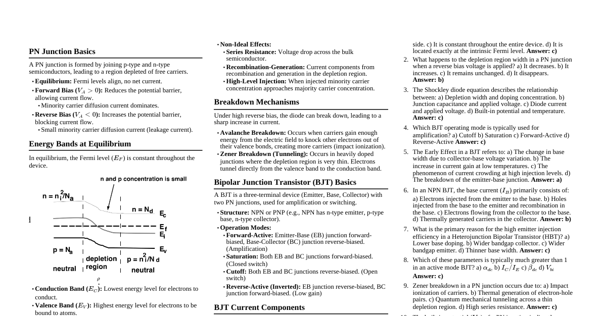
### Semiconductor Fundamentals - **Intrinsic Carrier Concentration ($n_i$):** - $n_i = \sqrt{N_c N_v} \exp\left(-\frac{E_g}{2kT}\right)$ - $N_c$: Effective density of states in conduction band. - $N_v$: Effective density of states in valence band. - $E_g$: Bandgap energy. - $kT$: Thermal energy ($0.0259 \text{ eV}$ at $300 \text{ K}$). - **Mass Action Law:** - $np = n_i^2$ (holds at thermal equilibrium) - **Carrier Concentrations (n-type, donor doping $N_D$):** - $n \approx N_D$ (majority carriers) - $p = \frac{n_i^2}{N_D}$ (minority carriers) - **Carrier Concentrations (p-type, acceptor doping $N_A$):** - $p \approx N_A$ (majority carriers) - $n = \frac{n_i^2}{N_A}$ (minority carriers) - **Fermi Level ($E_F$) for n-type:** - $E_F - E_i = kT \ln\left(\frac{N_D}{n_i}\right)$ - **Fermi Level ($E_F$) for p-type:** - $E_i - E_F = kT \ln\left(\frac{N_A}{n_i}\right)$ - $E_i$: Intrinsic Fermi level. - **Mobility ($\mu$):** - Carrier mobility describes how quickly an electron or hole moves in response to an electric field. - $\mu_n$: Electron mobility, $\mu_p$: Hole mobility. - Influenced by: - **Lattice scattering:** Dominant at high temperatures and low doping. - **Impurity scattering:** Dominant at low temperatures and high doping. - **Resistivity ($\rho$):** - $\rho = \frac{1}{q(n\mu_n + p\mu_p)}$ - For n-type: $\rho \approx \frac{1}{qN_D\mu_n}$ - For p-type: $\rho \approx \frac{1}{qN_A\mu_p}$ - **Current Density:** - **Drift Current:** Due to electric field. - $J_n^{drift} = qn\mu_n E$ - $J_p^{drift} = qp\mu_p E$ - **Diffusion Current:** Due to concentration gradient. - $J_n^{diff} = qD_n \frac{dn}{dx}$ - $J_p^{diff} = -qD_p \frac{dp}{dx}$ - Total current density: $J = J_n^{drift} + J_p^{drift} + J_n^{diff} + J_p^{diff}$ - **Einstein Relation:** - Relates diffusion coefficient ($D$) and mobility ($\mu$). - $\frac{D_n}{\mu_n} = \frac{D_p}{\mu_p} = \frac{kT}{q} = V_T$ (Thermal Voltage) - **Low-Level Injection:** - Condition where injected minority carrier concentration is much smaller than the majority carrier concentration. - Allows simplification of carrier transport equations. - **Recombination and Generation:** - **Recombination:** Electron and hole annihilate. - **Generation:** Electron-hole pair creation. - **Lifetime ($\tau$):** Average time a minority carrier exists before recombining. ### PN Junctions - **Formation & Equilibrium:** - Formed by joining p-type and n-type semiconductors. - At equilibrium, Fermi levels align, creating a built-in electric field and depletion region. - **Built-in Voltage ($V_{bi}$):** - $V_{bi} = \frac{kT}{q} \ln\left(\frac{N_A N_D}{n_i^2}\right)$ - Represents the potential barrier across the depletion region. - Higher doping concentrations lead to a larger $V_{bi}$. - **Depletion Region & Width ($W$):** - Region near the junction devoid of free carriers. - $W = \sqrt{\frac{2\epsilon_s}{q}\left(\frac{N_A+N_D}{N_A N_D}\right)(V_{bi} - V_A)}$ - $x_n = \sqrt{\frac{2\epsilon_s}{q}\frac{N_A}{N_D(N_A+N_D)}(V_{bi}-V_A)}$ (depletion width in n-side) - $x_p = \sqrt{\frac{2\epsilon_s}{q}\frac{N_D}{N_A(N_A+N_D)}(V_{bi}-V_A)}$ (depletion width in p-side) - $W = x_n + x_p$ - $\epsilon_s$: Permittivity of the semiconductor. - $V_A$: Applied voltage (positive for forward bias, negative for reverse bias). - Higher doping leads to a smaller depletion width. - **Junction Capacitance ($C_j$):** - Capacitance associated with the depletion region. - $C_j = \frac{\epsilon_s A}{W} = A\sqrt{\frac{q\epsilon_s}{2}\left(\frac{N_A N_D}{N_A+N_D}\right)\frac{1}{V_{bi}-V_A}}$ - $A$: Junction area. - Larger doping leads to larger junction capacitance (due to smaller $W$). - **Diode Current-Voltage (I-V) Characteristics (Shockley Equation):** - $I_D = I_S \left( e^{\frac{qV_A}{nkT}} - 1 \right)$ - $I_S$: Reverse saturation current. - $I_S = qA \left( \frac{D_p}{L_p} \frac{n_i^2}{N_D} + \frac{D_n}{L_n} \frac{n_i^2}{N_A} \right)$ - $L_p = \sqrt{D_p \tau_p}$, $L_n = \sqrt{D_n \tau_n}$ (diffusion lengths) - $n$: Ideality factor (typically 1 to 2). - **Forward Bias ($V_A > 0$):** Current increases exponentially. Minority carrier diffusion dominates. - **Reverse Bias ($V_A ### BJT Fundamentals - **Structure:** Three-terminal device (Emitter, Base, Collector) with two PN junctions. NPN or PNP. - **Operation Modes (for NPN):** - **Forward-Active (Amplification):** E-B forward biased, B-C reverse biased. - **Saturation (Closed Switch):** E-B forward biased, B-C forward biased. - **Cutoff (Open Switch):** E-B reverse biased, B-C reverse biased. - **Reverse-Active (Inverted, Low Gain):** E-B reverse biased, B-C forward biased. - **Minority Carrier Distribution (in Base, for NPN):** - In forward-active mode, minority electron concentration in the p-type base is approximately linear, decreasing from E-B junction to B-C junction. - **BJT Current Components (for NPN):** - **Emitter Current ($I_E$):** Total current entering emitter. $I_E = I_B + I_C$. - **Collector Current ($I_C$):** Current collected by collector. Primarily electrons from emitter diffused through base. - **Base Current ($I_B$):** Consists of: - Holes injected from base to emitter ($I_{Bp}$). - Electrons recombining in the base ($I_{BB}$). - Small leakage current from B-C junction ($I_{BC0}$). - **BJT Parameters:** - **Common Base Current Gain ($\alpha_{dc}$):** $\alpha_{dc} = \frac{I_C}{I_E}$ - Typically close to 1 (e.g., 0.95-0.99). - $\alpha_{dc} = \gamma \alpha_T$ - **Common Emitter Current Gain ($\beta_{dc}$):** $\beta_{dc} = \frac{I_C}{I_B}$ - Typically much greater than 1 (e.g., 50-200). - $\beta_{dc} = \frac{\alpha_{dc}}{1-\alpha_{dc}}$ - **Emitter Efficiency ($\gamma$):** Measures effectiveness of emitter in injecting minority carriers into base. - For NPN: $\gamma = \frac{I_{En}}{I_{En} + I_{Ep}}$ (where $I_{En}$ is electron current from emitter into base, $I_{Ep}$ is hole current from base into emitter). - To increase $\gamma$: high emitter doping relative to base doping, short emitter width. - **Base Transport Factor ($\alpha_T$):** Fraction of minority carriers injected into base that reach the collector. - To increase $\alpha_T$: narrow base width ($W_B$), long minority carrier lifetime in base ($\tau_B$). - **Non-Ideal Effects:** - **Base Width Modulation (Early Effect):** Effective base width changes with Collector-Base voltage $V_{CB}$, affecting $I_C$ and $\beta_{dc}$. - **Current Crowding:** At high currents, current tends to flow near the edges of the emitter. - **Breakdown:** Similar to PN junctions (avalanche or Zener). - **Heterojunction Bipolar Transistor (HBT):** - Uses different semiconductor materials (e.g., wider bandgap emitter, narrower bandgap base). - **Advantages:** Higher emitter injection efficiency (allows higher base doping for lower base resistance without sacrificing gain), improved frequency response. ### MOS Capacitor - **Structure:** Metal-Oxide-Semiconductor (MOS) structure. - **Metal Gate:** Electrode (e.g., aluminum, polysilicon). - **Oxide:** Insulating layer (e.g., $SiO_2$). - **Semiconductor Substrate:** (e.g., p-type Si). - **Capacitance-Voltage (C-V) Characteristics (for p-type substrate):** - **Accumulation ($V_{GS} V_T$):** - Positive gate voltage is strong enough to attract minority carriers (electrons) to the interface, forming an inversion layer. - **Low Frequency:** Inversion layer can respond to AC signal. $C \approx C_{ox}$. - **High Frequency:** Inversion layer cannot respond to AC signal. $C = \frac{C_{ox}C_{dep,max}}{C_{ox}+C_{dep,max}}$. (Capacitance remains at minimum, limited by maximum depletion width $W_{max}$). - **Flat Band Voltage ($V_{FB}$):** - The gate voltage at which the semiconductor is neither accumulated nor depleted. No band bending. - $V_{FB} = \phi_{ms} - \frac{Q_{ox}}{C_{ox}}$ - $\phi_{ms} = \phi_m - \phi_s = (\text{metal work function}) - (\text{semiconductor work function for intrinsic material})$ - $Q_{ox}$: Fixed oxide charge (often positive). - **Threshold Voltage ($V_T$) (for p-type substrate NMOS):** - The gate voltage required to create an inversion layer. - $V_T = V_{FB} + 2\phi_F + \frac{Q_{dep,max}}{C_{ox}}$ - $\phi_F = \frac{kT}{q} \ln\left(\frac{N_A}{n_i}\right)$ (Fermi potential for p-type semiconductor) - $Q_{dep,max} = -qN_A W_{max}$ (maximum depletion charge) - $W_{max} = \sqrt{\frac{2\epsilon_s (2\phi_F)}{qN_A}}$ (maximum depletion width) - **Oxide Capacitance ($C_{ox}$):** - $C_{ox} = \frac{\epsilon_{ox}}{t_{ox}}$ - $\epsilon_{ox}$: Permittivity of the oxide. - $t_{ox}$: Oxide thickness. ### MOSFET - **Structure:** Metal-Oxide-Semiconductor Field-Effect Transistor. - Source, Drain (heavily doped regions), Gate, Body/Substrate. - Channel formed at the $SiO_2$-Si interface between source and drain. - **NMOS vs. PMOS:** - **NMOS:** n-channel, uses p-type substrate. Conducts with positive $V_{GS}$. Majority carriers are electrons. - **PMOS:** p-channel, uses n-type substrate. Conducts with negative $V_{GS}$. Majority carriers are holes. - **Modes of Operation (for NMOS):** - **Cutoff ($V_{GS} V_T$ and $V_{DS} V_T$ and $V_{DS} \ge V_{GS} - V_T$):** - Channel is "pinched off" near the drain end. - $I_D = \frac{1}{2} \mu_n C_{ox} \frac{W}{L} (V_{GS}-V_T)^2 (1 + \lambda V_{DS})$ - Current becomes largely independent of $V_{DS}$. - $\lambda$: Channel length modulation parameter (accounts for slight increase in $I_D$ with $V_{DS}$). - MOSFET acts as a voltage-controlled current source. - **Threshold Voltage ($V_T$):** - The minimum gate-to-source voltage required to create a conductive channel. - **Enhancement-mode:** $V_T > 0$ (NMOS), $V_T 0$ (PMOS). Channel exists at $V_{GS}=0$. - **Transconductance ($g_m$):** - Measures the change in drain current with respect to gate-source voltage. - In saturation: $g_m = \frac{\partial I_D}{\partial V_{GS}} = \mu_n C_{ox} \frac{W}{L} (V_{GS}-V_T)$ - **Output Resistance ($r_o$):** - Measures the change in drain-source voltage with respect to drain current. - In saturation: $r_o = \left(\frac{\partial I_D}{\partial V_{DS}}\right)^{-1} = \frac{1}{\lambda I_D}$ (ignoring body effect). - **Body Effect:** - Change in threshold voltage due to voltage difference between source and body ($V_{SB}$). - $V_T = V_{T0} + \gamma (\sqrt{|2\phi_F + V_{SB}|} - \sqrt{|2\phi_F|})$ - $\gamma$: Body effect coefficient. ### MOS Practice Questions #### Question 1 (MOS Capacitor C-V) A MOS capacitor has a p-type silicon substrate with $N_A = 10^{16} \text{ cm}^{-3}$. The oxide thickness is $t_{ox} = 10 \text{ nm}$. Assume $\phi_{ms} = 0 \text{ V}$ and negligible fixed oxide charge. Calculate: 1. Oxide capacitance $C_{ox}$ (per unit area). 2. Flat-band voltage $V_{FB}$. 3. Threshold voltage $V_T$. **Given:** $\epsilon_s = 11.7 \epsilon_0$, $\epsilon_{ox} = 3.9 \epsilon_0$, $\epsilon_0 = 8.85 \times 10^{-14} \text{ F/cm}$, $q = 1.6 \times 10^{-19} \text{ C}$, $kT/q = 0.0259 \text{ V}$ at $300 \text{ K}$, $n_i = 10^{10} \text{ cm}^{-3}$. **Solution:** 1. **Oxide Capacitance ($C_{ox}$):** $C_{ox} = \frac{\epsilon_{ox}}{t_{ox}} = \frac{3.9 \times 8.85 \times 10^{-14} \text{ F/cm}}{10 \times 10^{-7} \text{ cm}} = 3.45 \times 10^{-7} \text{ F/cm}^2 = 3.45 \mu\text{F/cm}^2$ 2. **Flat-Band Voltage ($V_{FB}$):** Since $\phi_{ms} = 0 \text{ V}$ and $Q_{ox} = 0$, then $V_{FB} = 0 \text{ V}$. 3. **Threshold Voltage ($V_T$):** First, calculate $\phi_F$: $\phi_F = \frac{kT}{q} \ln\left(\frac{N_A}{n_i}\right) = 0.0259 \text{ V} \ln\left(\frac{10^{16}}{10^{10}}\right) = 0.0259 \text{ V} \ln(10^6) = 0.0259 \times 6 \ln(10) \approx 0.0259 \times 13.815 \approx 0.358 \text{ V}$ Next, calculate maximum depletion width $W_{max}$: $W_{max} = \sqrt{\frac{2\epsilon_s (2\phi_F)}{qN_A}} = \sqrt{\frac{2 \times 11.7 \times 8.85 \times 10^{-14} \text{ F/cm} \times (2 \times 0.358 \text{ V})}{1.6 \times 10^{-19} \text{ C} \times 10^{16} \text{ cm}^{-3}}}$ $W_{max} = \sqrt{\frac{7.40 \times 10^{-13}}{1.6 \times 10^{-3}}} = \sqrt{4.625 \times 10^{-10}} = 2.15 \times 10^{-5} \text{ cm} = 0.215 \mu\text{m}$ Then, calculate $Q_{dep,max}$: $Q_{dep,max} = -qN_A W_{max} = -1.6 \times 10^{-19} \text{ C} \times 10^{16} \text{ cm}^{-3} \times 2.15 \times 10^{-5} \text{ cm} = -3.44 \times 10^{-8} \text{ C/cm}^2$ Finally, calculate $V_T$: $V_T = V_{FB} + 2\phi_F + \frac{|Q_{dep,max}|}{C_{ox}} = 0 \text{ V} + 2 \times 0.358 \text{ V} + \frac{3.44 \times 10^{-8} \text{ C/cm}^2}{3.45 \times 10^{-7} \text{ F/cm}^2}$ $V_T = 0.716 \text{ V} + 0.0997 \text{ V} \approx 0.816 \text{ V}$ #### Question 2 (MOSFET I-V Characteristics) An NMOS transistor has $\mu_n C_{ox} = 100 \mu\text{A/V}^2$, $W/L = 10$, and $V_T = 0.5 \text{ V}$. Calculate the drain current $I_D$ for the following conditions: 1. $V_{GS} = 1 \text{ V}$, $V_{DS} = 0.2 \text{ V}$ 2. $V_{GS} = 1.5 \text{ V}$, $V_{DS} = 1 \text{ V}$ **Solution:** 1. **Condition 1:** $V_{GS} = 1 \text{ V}$, $V_{DS} = 0.2 \text{ V}$ First, check the operating region: $V_{GS} - V_T = 1 \text{ V} - 0.5 \text{ V} = 0.5 \text{ V}$ Since $V_{DS} (0.2 \text{ V}) ### Multiple Choice Questions #### MOS & MOSFET Questions **1. Which of the following statements is TRUE regarding the C-V characteristics of a MOS capacitor with a p-type substrate at high frequencies?** a) In accumulation, the capacitance is close to $C_{ox}$. b) In strong inversion, the capacitance is equal to $C_{ox}$. c) As the gate voltage increases from accumulation to depletion, the capacitance increases. d) The minimum capacitance occurs in accumulation. **Answer: a)** *Explanation:* In accumulation, holes accumulate at the semiconductor surface, and the capacitance is dominated by the oxide capacitance. In strong inversion at high frequencies, the inversion layer cannot respond to the AC signal, so the capacitance remains at its minimum value (determined by $C_{ox}$ and $C_{dep,max}$). **2. For an NMOS transistor operating in the saturation region, which parameter primarily controls the drain current ($I_D$)?** a) $V_{DS}$ b) $V_{GS}$ c) Channel length $L$ d) Substrate doping concentration $N_A$ **Answer: b)** *Explanation:* In saturation, the drain current is primarily controlled by $V_{GS}$ through the $(V_{GS}-V_T)^2$ term, making the MOSFET act as a voltage-controlled current source. $V_{DS}$ has a minor effect due to channel length modulation, but $V_{GS}$ is the dominant control. **3. Increasing the oxide thickness ($t_{ox}$) in a MOS capacitor will generally lead to:** a) An increase in $C_{ox}$ and a decrease in $V_T$. b) A decrease in $C_{ox}$ and an increase in $V_T$. c) An increase in $C_{ox}$ and an increase in $V_T$. d) A decrease in $C_{ox}$ and a decrease in $V_T$. **Answer: b)** *Explanation:* $C_{ox} = \frac{\epsilon_{ox}}{t_{ox}}$, so increasing $t_{ox}$ decreases $C_{ox}$. $V_T = V_{FB} + 2\phi_F + \frac{Q_{dep,max}}{C_{ox}}$. If $C_{ox}$ decreases, the $\frac{Q_{dep,max}}{C_{ox}}$ term increases, leading to an increase in $V_T$. **4. What is the condition for an NMOS transistor to be in the linear (triode) region?** a) $V_{GS} V_T$ and $V_{DS} \ge V_{GS} - V_T$ c) $V_{GS} > V_T$ and $V_{DS} V_T$) and the channel is not pinched off ($V_{DS}