BJT Transistors & Amplifiers
Cheatsheet Content
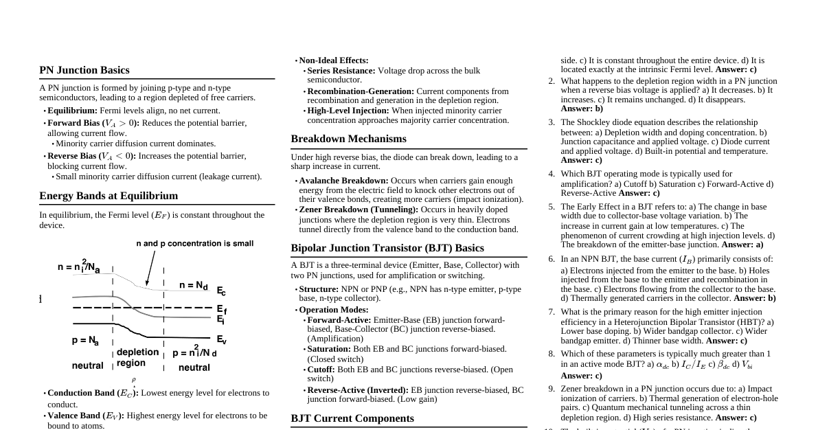
### BJT Fundamentals - **Bipolar Junction Transistor (BJT):** A three-terminal semiconductor device (Emitter, Base, Collector) with two p-n junctions. - **Types:** - **NPN:** Two N-type regions separated by a P-type region. - **PNP:** Two P-type regions separated by an N-type region. - **Junctions:** - Base-Emitter (BE) junction - Base-Collector (BC) junction #### BJT Currents - **Emitter Current ($I_E$):** Sum of collector and base currents. $$I_E = I_C + I_B$$ - **DC Current Gain ($\beta_{DC}$ or $h_{FE}$):** Ratio of collector current to base current. $$\beta_{DC} = \frac{I_C}{I_B}$$ - **Alpha ($\alpha_{DC}$):** Ratio of collector current to emitter current. $$\alpha_{DC} = \frac{I_C}{I_E}$$ (Typically $\alpha_{DC} \approx \beta_{DC} / (\beta_{DC} + 1)$) **Video Resource:** [NPN and PNP Transistors Explained](https://www.youtube.com/watch?v=A3UjPzL28t8) ### BJT Biasing - **Purpose:** To set the transistor's DC operating point (Q-point) for linear amplification. - **Normal Operation (Active Region):** - **NPN:** Base-Emitter (BE) junction is forward-biased (Base > Emitter), Base-Collector (BC) junction is reverse-biased (Collector > Base). - **PNP:** Base-Emitter (BE) junction is forward-biased (Emitter > Base), Base-Collector (BC) junction is reverse-biased (Base > Collector). #### Regions of Operation - **Saturation Region:** Both BE and BC junctions are forward-biased. Transistor acts like a closed switch. - **Active Region:** BE forward-biased, BC reverse-biased. Used for amplification. - **Cutoff Region:** Both BE and BC junctions are reverse-biased. Transistor acts like an open switch (no current flow). - **Breakdown Region:** Occurs at high voltages, leading to rapid current increase and potential transistor damage. **Video Resource:** [Transistor Biasing Basics](https://www.youtube.com/watch?v=F0f54sW-1iM) ### Collector Characteristic Curves - Plot of $I_C$ vs. $V_{CE}$ for various $I_B$ values. - Shows the relationship between collector current, collector-emitter voltage, and base current. *Example of Collector Characteristic Curves for an NPN BJT, showing saturation, active, and breakdown regions.* ### Load Lines - A graphical method to determine the Q-point. - Represents the DC operating path of the external circuit connected to the transistor. #### Constructing a DC Load Line 1. **Find $I_C$ (max):** Set $V_{CE} = 0$. $I_C = V_{CC} / R_C$. (Y-intercept) 2. **Find $V_{CE}$ (max):** Set $I_C = 0$. $V_{CE} = V_{CC}$. (X-intercept) 3. Draw a line between these two points on the $I_C$ vs. $V_{CE}$ graph. #### Q-point (Quiescent Point) - The intersection of the load line with the appropriate $I_B$ characteristic curve. - Represents the DC operating point ($I_{CQ}$, $V_{CEQ}$). **Video Resource:** [DC Load Line and Q-point](https://www.youtube.com/watch?v=Q74V3Nq0N0g) ### Small Signal Model - Used for analyzing the AC behavior of transistors. - Linearizes the transistor's non-linear characteristics around the Q-point. #### Key Parameters - **Transconductance ($g_m$):** Relates change in collector current to change in base-emitter voltage. $$g_m = \frac{\Delta I_C}{\Delta V_{BE}} \approx \frac{I_C}{V_T}$$ where $V_T$ (thermal voltage) $\approx 25 \text{mV}$ at room temperature. - **Input Resistance ($r_\pi$):** AC resistance looking into the base. $$r_\pi = \frac{\Delta V_{BE}}{\Delta I_B} \approx \frac{\beta_{AC}}{g_m}$$ or $$r_\pi = \beta_{AC} r_e$$ - **Emitter Resistance ($r_e$):** AC resistance of the emitter diode. $$r_e = \frac{1}{g_m} \approx \frac{V_T}{I_E}$$ **Video Resource:** [BJT Small-Signal Model (Hybrid-Pi)](https://www.youtube.com/watch?v=h_4lUj9R9bY) ### Transistor Biasing Circuits #### 1. Base Bias - **Circuit:** Simple, uses a single resistor ($R_B$) to set $I_B$. - **Equations:** $$I_B = \frac{V_{CC} - V_{BE}}{R_B}$$ $$I_C = \beta_{DC} I_B$$ $$V_{CE} = V_{CC} - I_C R_C$$ - **Disadvantage:** Q-point is highly dependent on $\beta_{DC}$, which varies significantly between transistors and with temperature. Not a good design for stable operation. #### 2. Voltage-Divider Bias (Self-Bias) - **Circuit:** Uses two resistors ($R_1$, $R_2$) to create a stable base voltage ($V_B$). - **Approximation (if $R_2 \ll \beta_{DC} R_E$):** $$V_B = V_{CC} \frac{R_2}{R_1 + R_2}$$ $$V_E = V_B - V_{BE}$$ $$I_E = \frac{V_E}{R_E}$$ $$I_C \approx I_E$$ $$V_C = V_{CC} - I_C R_C$$ $$V_{CE} = V_C - V_E$$ - **Advantage:** Provides a stable Q-point largely independent of $\beta_{DC}$ variations. **Video Resource:** [Voltage Divider Bias Explained](https://www.youtube.com/watch?v=W61_67z878k) ### Common-Emitter (CE) Amplifier - **Configuration:** Input applied to base, output taken from collector. Emitter is AC ground (often bypassed). - **Characteristics:** - High voltage gain. - Output is $180^\circ$ out of phase with the input (inverted). #### AC Model *Simplified AC equivalent circuit for a CE amplifier.* #### Voltage Gain ($A_V$) - For a CE amplifier with an unbypassed emitter resistor $R_E$: $$A_V = \frac{V_{out}}{V_{in}} \approx -\frac{R_C}{r_e + R_E}$$ - For a CE amplifier with a fully bypassed emitter resistor (AC ground): $$A_V = \frac{V_{out}}{V_{in}} \approx -\frac{R_C}{r_e}$$ #### Input Resistance ($R_{in(tot)}$) - Total input resistance seen by the signal source. - Includes biasing resistors ($R_1 || R_2$) and the transistor's input resistance ($\beta_{AC} r_e$). $$R_{in(tot)} = R_1 || R_2 || (\beta_{AC} (r_e + R_E'))$$ (where $R_E'$ is the unbypassed portion of $R_E$) #### Coupling and Bypass Capacitors - **Coupling Capacitors ($C_1, C_2$):** Block DC, allow AC signal to pass. - **Bypass Capacitor ($C_3$):** Provides an AC short across $R_E$ to increase AC gain without affecting DC bias. **Video Resource:** [Common Emitter Amplifier Analysis](https://www.youtube.com/watch?v=VzZp0c_pB4I) ### Capacitor Sizing - Capacitors define the low-frequency response of the amplifier. - The -3dB frequency ($f_{-3dB}$) for a given RC circuit: $$f_{-3dB} = \frac{1}{2 \pi R C}$$ - **Input Coupling Capacitor ($C_{in}$):** Sets the lower cutoff frequency with the input resistance ($R_{in(tot)}$). $$C_{in} = \frac{1}{2 \pi R_{in(tot)} f_{-3dB(in)}}$$ - **Output Coupling Capacitor ($C_{out}$):** Sets the lower cutoff frequency with the output load resistance. - **Bypass Capacitor ($C_E$):** Sets the lower cutoff frequency with the emitter resistance ($R_E || r_e$). **Video Resource:** [RC Filter Cutoff Frequency](https://www.youtube.com/watch?v=0kFpW0809Gk) ### BJT as a Switch - BJTs can operate as electronic switches by alternating between cutoff and saturation regions. - **Cutoff (OFF state):** - Input voltage is low (e.g., $V_{in} I_{B(min\_sat)} = I_{C(sat)} / \beta_{DC}$. - Transistor acts as a closed switch. - $V_{out} \approx V_{CE(sat)}$ (typically $0.1 \text{V}$ to $0.3 \text{V}$). **Video Resource:** [Transistor as a Switch](https://www.youtube.com/watch?v=FjI1Vv1-0pY)