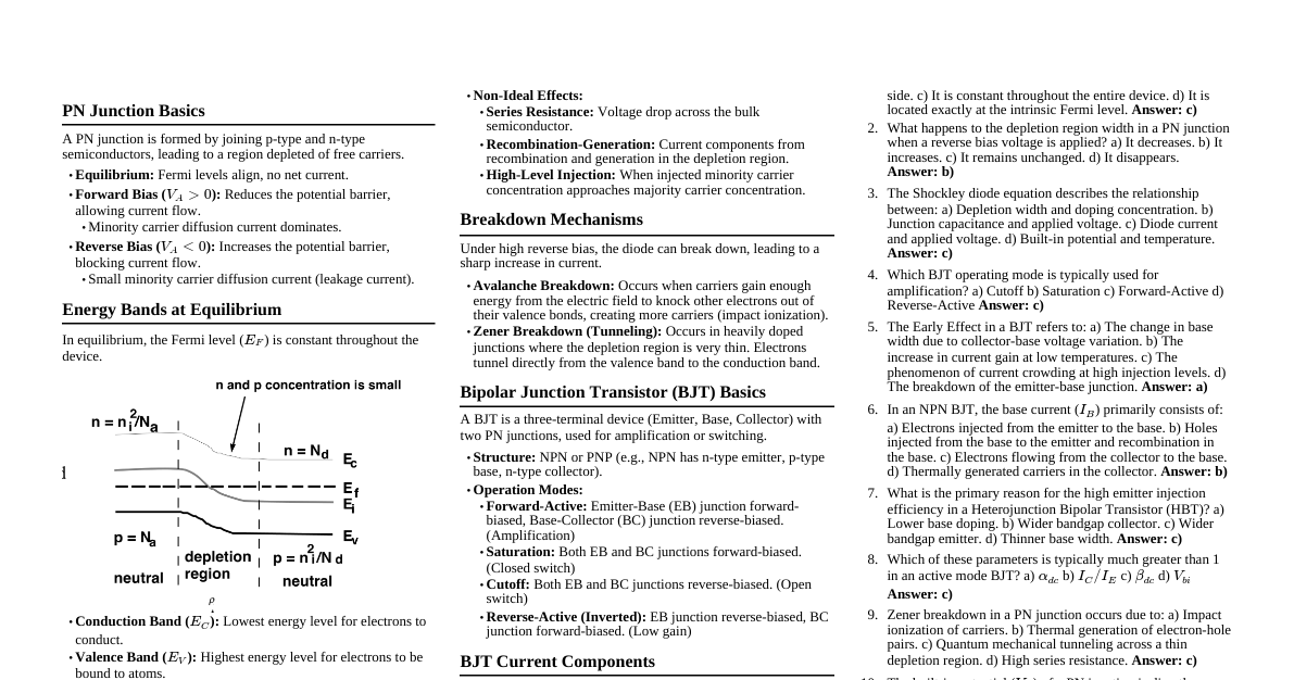
BJT in CE Configuration
Cheatsheet Content
Transistor Construction Three-terminal device: Base (B), Emitter (E), Collector (C). Operates in common base, common emitter, or common collector configurations. Can be used for voltage and current amplification. Has two p-n junctions. Input signal applied to the base, magnified output signal at the collector. Bipolar Junction Transistor (BJT) Operation depends on both majority and minority carriers, hence "bipolar". "Transistor" comes from "Transfer" and "Resistor". Amplification achieved by passing input current from low resistance region to high resistance region. Concept of "TRANSfer-resISTOR" gives the name. Types of BJTs NPN Transistor: Emitter (n-type), Base (p-type), Collector (n-type). PNP Transistor: Emitter (p-type), Base (n-type), Collector (p-type). Doping Levels Emitter: Heavily doped (e.g., $10^{15}$ impurities). Supplies charge carriers. Base: Lightly doped (e.g., $10^9$ impurities). Controls charge carrier flow. Collector: Moderately doped (e.g., $10^7 - 10^8$ impurities). Collects charge carriers. Transistor Junctions Emitter-Base Junction (EBJ): Between emitter and base. Collector-Base Junction (CBJ): Between collector and base. Biasing of Transistor For proper operation, the two junctions must have correct DC bias voltages: Base-Emitter (BE) junction must be forward biased . Base-Collector (BC) junction must be reverse biased . Modes of Transistor Operation Mode EB Junction CB Junction Behavior Active Region Forward Biased Reverse Biased Amplifier, analog circuits Cut-off Region Reverse Biased Reverse Biased Open switch, nearly zero current Saturation Region Forward Biased Forward Biased Closed switch, large collector current NPN Transistor Operation Forward bias $V_{EE}$ reduces depletion region at EBJ. Reverse bias $V_{CC}$ increases depletion region at CBJ. Forward bias causes electrons from emitter to base. Base is lightly doped p-type, so few holes combine with electrons (base current). Remaining electrons cross over to collector (collector current). Collector current is larger than base current. Emitter current: $I_E = I_B + I_C$ PNP Transistor Operation Forward bias $V_{EE}$ reduces depletion region at EBJ. Reverse bias $V_{CC}$ increases depletion region at CBJ. Forward bias causes holes from emitter to base. Base is lightly doped n-type, so few electrons combine with holes (base current). Remaining holes cross over to collector (collector current). Collector current is larger than base current. Emitter current: $I_E = I_B + I_C$ Transistor Circuit Configurations Three types based on common electrode: Common Base (CB): Grounded base. Common Emitter (CE): Grounded emitter. Common Collector (CC): Grounded collector. The common electrode is shared by input and output circuits and is generally grounded. Common Emitter (CE) Configuration Emitter is common to both input and output signals. Input signal applied between base and emitter. Output taken between collector and emitter. Produces highest current and power gain among all BJT configurations. Input impedance: LOW (due to forward-biased PN-junction). Output impedance: HIGH (due to reverse-biased PN-junction). Used when large current gain is needed, bias stabilization, audio frequency applications. CE Input Characteristics Describes relationship between input current ($I_B$) and input voltage ($V_{BE}$). $I_B$ on y-axis, $V_{BE}$ on x-axis. To determine, $V_{CE}$ is kept constant (e.g., 0V, 10V, 20V) and $V_{BE}$ is increased. For each $V_{BE}$, corresponding $I_B$ is recorded. When $V_{CE}=0V$ and EBJ is forward biased, it acts like a normal p-n diode. After 0.7V, a small increase in $V_{BE}$ rapidly increases $I_B$. In CE, $I_B$ is small due to lightly doped, narrow base. In CB, input current ($I_E$) is large due to heavily doped, wide emitter. Input current in CE is in microamperes ($\mu A$), in CB in milliamperes ($mA$). EBJ is forward biased, CBJ is reverse biased. Depletion region at EBJ is small, at CBJ is large. Increasing $V_{CE}$ further increases depletion region width. Base region is lightly doped, so depletion region penetrates more into base. This reduces input current ($I_B$). For higher $V_{CE}$, the curve shifts right, increasing cut-in voltage above 0.7V. CE Output Characteristics Describes relationship between output current ($I_C$) and output voltage ($V_{CE}$). $I_C$ on y-axis, $V_{CE}$ on x-axis. To determine, input current ($I_B$) is kept constant (e.g., $0 \mu A, 20 \mu A, \dots$) and $V_{CE}$ is increased. For each $V_{CE}$, corresponding $I_C$ is recorded. Regions of Operation (CE Output Characteristics) Cut-off region: When $I_B = 0 \mu A$, both junctions are reverse biased. Active region: Emitter-base junction forward biased, collector-base junction reverse biased. This is where amplification occurs. Saturation region: When $V_{CE}$ is reduced to a small value (e.g., 0.2V), CBJ becomes forward biased. Both junctions forward biased. Small increase in $V_{CE}$ rapidly increases $I_C$. Transistor Parameters Forward Current Gain / Current Amplification Factor ($\beta$) Ratio of output current (collector) to input current (base). $$ \beta = \frac{I_C}{I_B} $$ High in CE configuration, used for current amplification. Reverse Voltage Gain ($h_{re}$) Ratio of change in input (base) voltage to change in output (collector) voltage. $$ h_{re} = \frac{\Delta V_{BE}}{\Delta V_{CE}} \quad \text{at constant } I_B $$ Dynamic Input Resistance ($r_i$) Ratio of change in input voltage ($V_{BE}$) to change in input current ($I_B$) at constant output voltage ($V_{CE}$). $$ r_i = \frac{\Delta V_{BE}}{\Delta I_B} \quad \text{at constant } V_{CE} $$ Very low in CE configuration. Dynamic Output Resistance ($r_o$) Ratio of change in output voltage ($V_{CE}$) to change in output current ($I_C$) at constant input current ($I_B$). $$ r_o = \frac{\Delta V_{CE}}{\Delta I_C} \quad \text{at constant } I_B $$ High in CE configuration. Relation between $\beta$ and $\alpha$ (Common Base Current Gain) Given: $I_E = I_B + I_C$ Common Base current gain $\alpha = \frac{\Delta I_C}{\Delta I_E}$ Common Emitter current gain $\beta = \frac{\Delta I_C}{\Delta I_B}$ Relationship: $$ \beta = \frac{\alpha}{1 - \alpha} $$ Collector Current ($I_C$) Equation The total collector current ($I_C$) is given by: $$ I_C = \beta I_B + I_{CEO} $$ where $I_{CEO}$ is the collector-emitter leakage current with base open ($I_B = 0$). $$ I_{CEO} = \frac{1}{1-\alpha} I_{CBO} $$ where $I_{CBO}$ is the collector-base leakage current with emitter open. Applications of BJT in CE Configuration Amplification of small amplitude signals. Used in amplifier and oscillator circuits. Used as a switch in digital circuits. Wide applicability in electronic equipment like mobile phones, industrial control, television, radio transmitters, computers, satellites.