Diode Cheat Sheet
Cheatsheet Content
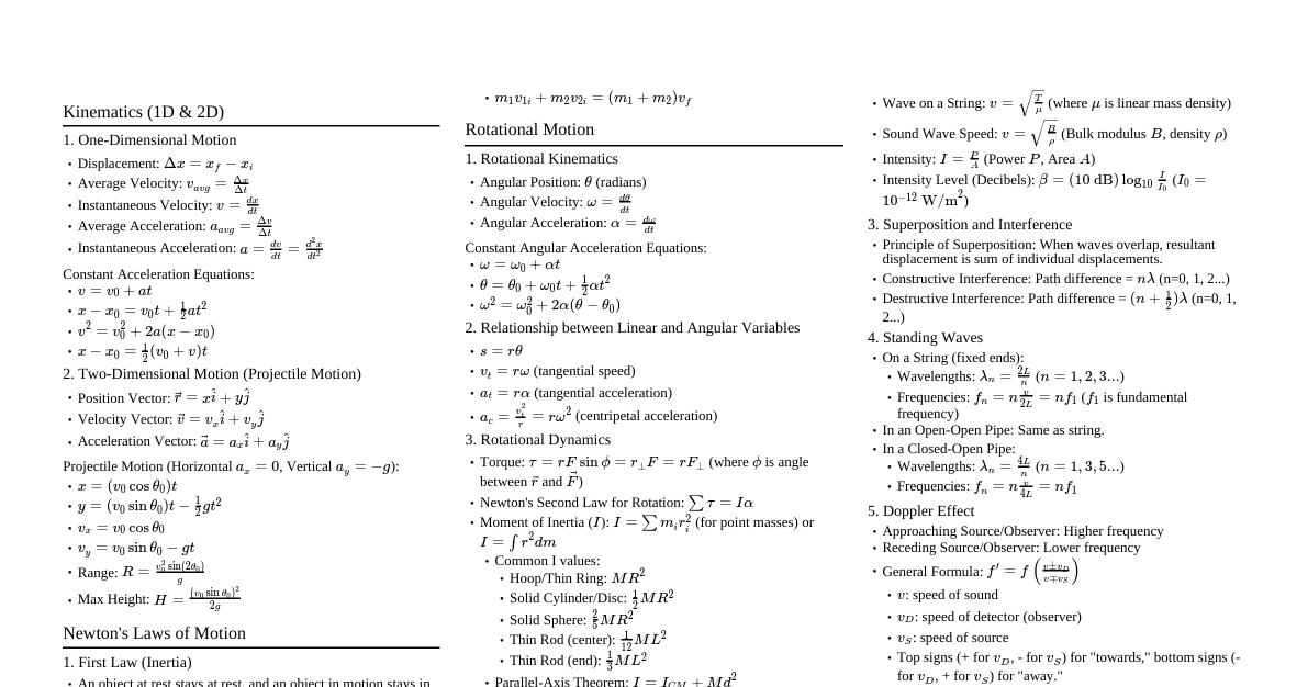
### PN Junction Diode Fundamentals - **PN Junction Formation:** Formed by joining p-type (excess holes) and n-type (excess electrons) semiconductors. - **Forward Bias:** Positive voltage applied to p-side, negative to n-side. Reduces depletion region, allows current flow. - **Reverse Bias:** Negative voltage applied to p-side, positive to n-side. Increases depletion region, blocks current flow (ideally). - **Depletion Region:** Area near junction devoid of free charge carriers due to diffusion across the junction, creating an electric field. - **Reverse Saturation Current ($I_S$):** Small, temperature-dependent current that flows under reverse bias due to minority carriers. - **Diode Current Components:** Diffusion current (major in forward bias), drift current (major in reverse bias). - **Cut-in Voltage ($V_{cut-in}$):** Minimum forward voltage required for significant current flow (e.g., ~0.7V for Si, ~0.3V for Ge). - **V-I Characteristics:** Exponential current increase in forward bias, very small current in reverse bias until breakdown. - **Diode Equation (Shockley):** $$I_D = I_S \left( e^{\frac{V_D}{\eta V_T}} - 1 \right)$$ - $I_D$: Diode current - $I_S$: Reverse saturation current - $V_D$: Diode voltage - $\eta$: Ideality factor (1 for Ge, 1-2 for Si) - $V_T$: Thermal voltage ($kT/q \approx 26mV$ at room temp) - **Temperature Effects:** - $I_S$ increases significantly with temperature. - $V_{cut-in}$ decreases by ~2mV/°C for Si. - Breakdown voltage increases. ### Diode Models - **Ideal Diode Model:** - Forward Bias: Short circuit ($V_D = 0$, $I_D > 0$) - Reverse Bias: Open circuit ($I_D = 0$, $V_D 0$) - Reverse Bias: Open circuit ($I_D = 0$, $V_D ### Zener Diode - **Zener Breakdown:** Occurs in heavily doped diodes at low reverse voltages. High electric field causes electrons to tunnel from valence to conduction band. - **Avalanche Breakdown:** Occurs in lightly doped diodes at higher reverse voltages. High electric field accelerates minority carriers, causing collisions and creation of more electron-hole pairs. - **Zener Characteristics:** Exhibits a sharp, stable breakdown voltage ($V_Z$) in reverse bias, making it useful for voltage regulation. - **Shunt Voltage Regulator:** Zener diode connected in parallel (shunt) with the load to maintain a constant output voltage. - **Regulator Design:** - Choose $V_Z$ equal to desired output voltage. - Select series resistor $R_S$ to limit current and drop excess voltage. - Ensure $I_Z \ge I_{Zmin}$ (minimum Zener current) and $P_Z \le P_{Zmax}$ (maximum power dissipation). ### Special Diodes - **Schottky Diode:** Metal-semiconductor junction. Lower forward voltage drop, faster switching speed than PN junction diodes. - **Tunnel Diode:** Heavily doped PN junction, exhibits negative resistance region due to quantum tunneling. Used in high-frequency oscillators. - **LED (Light Emitting Diode):** Emits light when forward biased due to recombination of electrons and holes. - **Varactor Diode (Variable Capacitance Diode):** PN junction whose capacitance varies with reverse bias voltage. Used in VCOs (Voltage Controlled Oscillators). ### Rectifiers - **Half-Wave Rectifier:** Allows only half of the AC input waveform to pass. - Output: Pulsating DC. - $$V_{DC} = \frac{V_m}{\pi}$$ - $$f_{ripple} = f_{in}$$ - **Full-Wave (Center-Tap) Rectifier:** Uses a center-tapped transformer and two diodes to rectify both halves of the AC waveform. - Output: Pulsating DC. - $$V_{DC} = \frac{2V_m}{\pi}$$ - $$f_{ripple} = 2f_{in}$$ - **Bridge Rectifier:** Uses four diodes to rectify both halves of the AC waveform without a center-tapped transformer. - Output: Pulsating DC. - $$V_{DC} = \frac{2V_m}{\pi}$$ - $$f_{ripple} = 2f_{in}$$ - **PIV (Peak Inverse Voltage):** Maximum reverse voltage a diode must withstand. - Half-Wave: $V_m$ - Full-Wave (Center-Tap): $2V_m$ - Bridge: $V_m$ - **Efficiency ($\eta$):** Ratio of DC output power to AC input power. - Half-Wave: 40.6% - Full-Wave: 81.2% - **Ripple Factor ($\gamma$):** Measure of AC variation in DC output. Lower is better. - Half-Wave: 1.21 - Full-Wave: 0.482 ### Rectifier with Filters - **Capacitor Filter:** Capacitor connected in parallel with the load at the rectifier output. Charges during peak voltage, discharges during ripple valley, smoothing the DC output. - **Ripple Reduction:** Capacitor reduces the ripple voltage by storing charge. Larger capacitance reduces ripple more effectively. - **Output DC Voltage with Filter:** - For full-wave with capacitor filter: $$V_{DC} \approx V_m - \frac{I_{DC}}{4 f C}$$ - Ripple voltage (peak-to-peak): $$V_{r(pp)} \approx \frac{V_m}{f_{ripple} R_L C}$$ ### Wave-Shaping Circuits #### Clippers - **Clippers:** Circuits that remove portions of an input signal above or below a certain voltage level. - **Series Clipper:** Diode in series with the signal path. - **Shunt Clipper:** Diode in parallel with the signal path. - **Biased Clipper:** Uses a DC voltage source to set the clipping level. #### Clampers - **Clampers (DC Restorers):** Shift the DC level of an AC signal without altering its waveform. Require a capacitor, diode, and resistor. - **Positive Clamper:** Shifts the waveform up so that its negative peak is clamped to a reference voltage (often 0V). - **Negative Clamper:** Shifts the waveform down so that its positive peak is clamped to a reference voltage (often 0V). - **Biased Clamper:** Uses a DC voltage source to clamp the peak to a non-zero voltage. ### Voltage Multipliers - **Voltage Multipliers:** Circuits that produce a DC output voltage that is a multiple of the peak input AC voltage. - **Doubler (Half-Wave):** Uses two diodes and two capacitors to produce an output approximately $2V_m$. - **Tripler:** Uses three diodes and three capacitors to produce an output approximately $3V_m$. - **Quadrupler:** Uses four diodes and four capacitors to produce an output approximately $4V_m$.